Intel Launches 4S and 8S Broadwell-EX Xeons: E7-4800 v4 and E7-8800 v4 Families, up to 384 Threads
by Ian Cutress on June 13, 2016 8:30 AM EST- Posted in
- CPUs
- Intel
- Xeon
- Enterprise
- v4
- Broadwell
- Broadwell-EX
- E7
- E7 v4

The super-high-end of Intel’s Xeon CPU range, based on servers with as many cores and as much memory as you can throw at them, represent a good part of Intel’s business with the potential to offer large margins: some customers want the most, the best, the powerful, and are willing to pay for it. For a number of generations, this has come via the Intel E7 line, consisting of two families of products designed for quad-socket servers (the E7-4000 v4) and eight socket servers (the E7-8000 v4). The new element to this launch is the use of ‘v4’, meaning that following the launch of Broadwell-EP for 1S/2S systems a couple of months ago and Broadwell-E (high-end desktop, HEDT) two weeks go, Intel has now filled out the v4 product line as we would typically expect. The new Xeons will be under the Broadwell-EX nomenclature (following Haswell-EX, Ivy Bridge-EX and so on), and using the Brickland platform aimed at mission critical environments.
Intel currently runs several processor lines in the Xeon/enterprise space, from E3-1200 v5 processors using consumer level performance in a Xeon package, the recently released E3-1500 v5 processors with embedded DRAM to help accelerate visual/video workflow, all the way up to the large EX core platforms.
| Intel Xeon Families (June 2016) | |||||
| E3-1200 v5 | E3-1500 v5 E3-1500M v5 |
E5-1600 v4 E5-2600 v4 |
E7-4800 v4 | E7-8800 v4 | |
| Core Family | Skylake | Skylake | Broadwell | Broadwell | Broadwell |
| Core Count | 2 to 4 | 2 to 4 | 4 to 22 | 8 to 16 | 4 to 24 |
| Integrated Graphics | Few, HD 520 | Yes, Iris Pro | No | No | No |
| DRAM Channels | 2 | 2 | 4 | 4 | 4 |
| Max DRAM Support (per CPU) | 64 GB | 64 GB | 1536 GB | 3072 GB | 3072GB |
| DMI/QPI | DMI 3.0 | DMI 3.0 | 2600: 1xQPI | 3 QPI | 3 QPI |
| Multi-Socket Support | No | No | 2600: 1S or 2S | 1S, 2S or 4S | Up to 8S |
| PCIe Lanes | 16 | 16 | 40 | 32 | 32 |
| Cost | $213 to $612 |
$396 to $1207 |
$294 to $4115 |
$1223 to $3003 |
$4061 to $7174 |
| Suited For | Entry Workstations | QuickSync, Memory Compute |
High-End Workstation | Many-Core Server | World Domination |
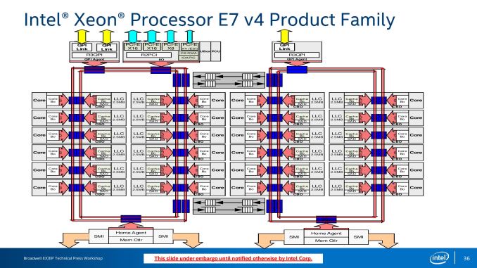
As referred to in Johan’s very detailed review of the dual socket E5-2600 v4 platform, Broadwell Xeon processor dies come in three die sizes: a low core count (LCC) featuring ten physical cores at 246.24 mm2 for ~3.2 billion transistors, a medium core count (MCC) with fifteen physical cores at 306.18 mm2 for ~4.7 billion transistors, and high core count (HCC) with 24 physical cores at 456.12mm2 for ~7.2 transistors. The MCC and HCC arrangements use dual memory controllers to address four memory channels whereas the LCC die uses a single memory controller which results in a slight performance hit compared to the other two. Most of the new E7 v4 processors however will be using the HCC die.
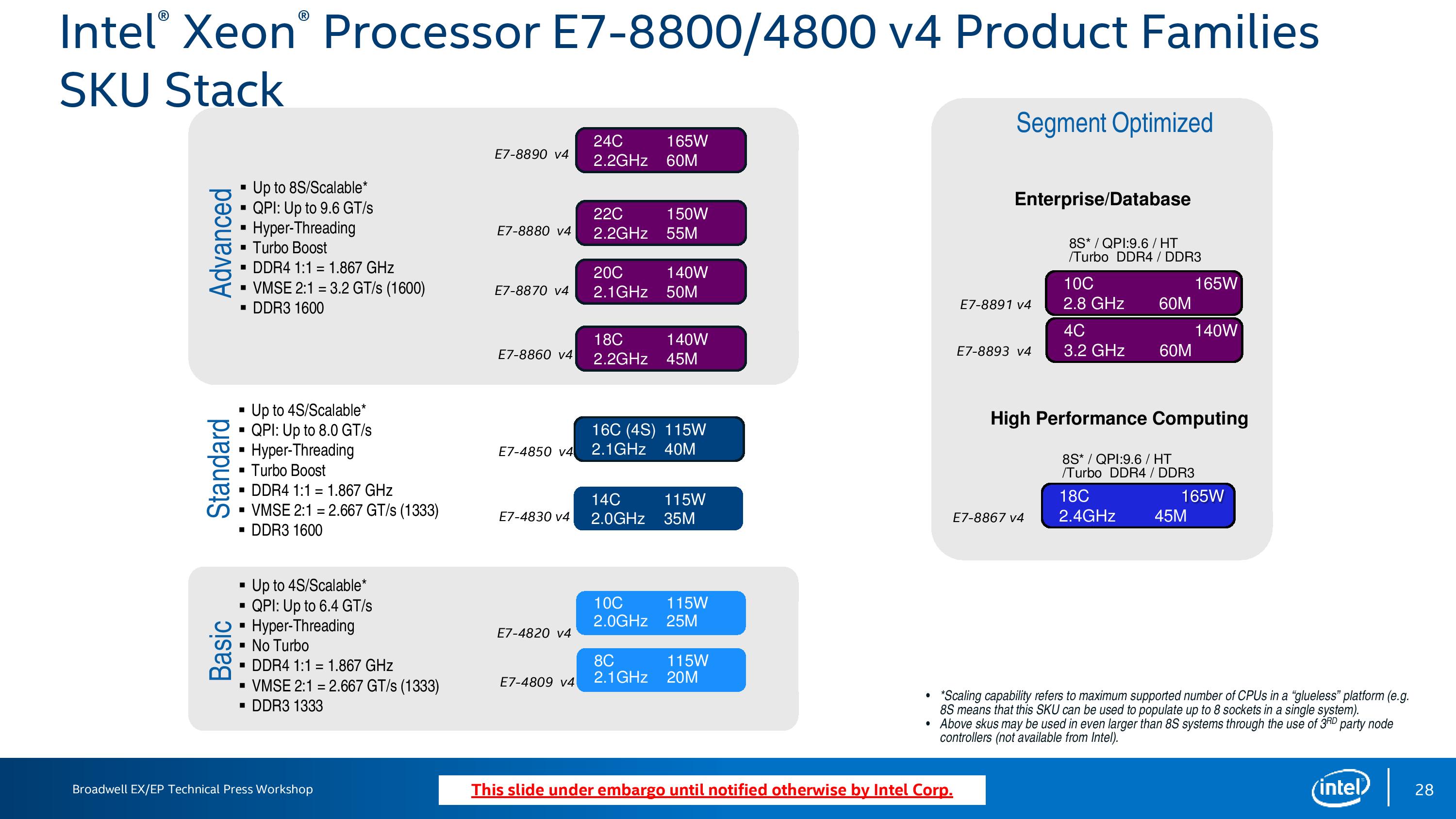
Intel has formally announced eleven processors between the 4S and 8S families, varying in core count, frequency, power consumption and L3 cache. The design of the HCC core is such that a processor can have certain cores fused off but the rest of the die can have access to the L3 cache, providing some SKUs with more ‘total cache per core’, such as the E7-8893 v4 which will be a four-core design but with 60 MB of L3 cache between them. These are classified by Intel as 'segment optimized', where applications require faster cache rather than more cores. This is arguably a stone-throw away from an eDRAM SKU with 64MB of eDRAM, but in this case Intel is still going with a large (and faster than eDRAM) L3 cache.
| Intel E7-8800 v4 Xeon Family | ||||||||
| E7-8860 v4 | E7-8867 v4 | E7-8870 v4 | E7-8880 v4 | E7-8890 v4 | E7-8891 v4 | E7-8893 v4 | ||
| TDP | 140 W | 165 W | 140 W | 150 W | 165 W | 165 W | 140 W | |
| Cores | 18 / 36 | 18 / 36 | 20 / 40 | 22 / 44 | 24 / 48 | 10 / 20 | 4 / 8 | |
| Base (MHz) | 2200 | 2400 | 2100 | 2200 | 2200 | 2800 | 3200 | |
| Turbo (MHz) | 3200 | 3300 | 3000 | 3300 | 3400 | 3500 | 3500 | |
| L3 Cache | 45 MB | 45 MB | 50 MB | 55 MB | 60 MB | 60 MB | 60 MB | |
| QPI (GT/s) | 3 x 9.6 | 3 x 9.6 | 3 x 9.6 | 3 x 9.6 | 3 x 9.6 | 3 x 9.6 | 3 x 9.6 | |
| DRAM Support | DDR4-1866 DDR3-1600 |
DDR4-1866 DDR3-1600 |
||||||
| PCIe Support | 3.0 x32 | 3.0 x32 | 3.0 x32 | 3.0 x32 | 3.0 x32 | 3.0 x32 | 3.0 x32 | |
| Price | $4061 | $4672 | $4762 | $5895 | $7174 | $6841 | $6841 | |
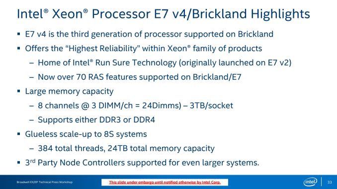
The flagship model is the E7-8890 v4, a 165W processor supporting the full 24 cores in the HCC die with hyperthreading, offering 48 threads per CPU. At a base frequency of 2.2 GHz, this processor can be used in an eight-socket glueless configuration (an 8S implementation means 192 cores/384 threads) or up to 128 sockets using third party controllers. In the eight socket configuration, a system can support up to 24TB of DDR4 LRDIMMs (three modules per channel, 12 modules per socket, 256GB per module). All the CPUs listed will support DDR4 and DDR3 with the dual controller configuration.
| Intel E7-4800 v4 Xeon Family | ||||
| E7-4809 v4 | E7-4820 v4 | E7-4830 v4 | E7-4850 v4 | |
| TDP | 115 W | 115 W | 115 W | 115 W |
| Cores | 8 / 16 | 10 / 20 | 14 / 28 | 16 / 32 |
| Base (MHz) | 2100 | 2000 | 2000 | 2100 |
| Turbo (MHz) | - | - | 2800 | 2800 |
| L3 Cache | 20 MB | 25 MB | 35 MB | 40MB |
| QPI (GT/s) | 3 x 6.4 | 3 x 6.4 | 3 x 8.0 | 3 x 8.0 |
| DRAM Support | DDR4-1866 DDR3-1600 |
|||
| PCIe Support | 3.0 x32 | 3.0 x32 | 3.0 x32 | 3.0 x32 |
| Price | $1223 | $1502 | $2170 | $3003 |
The E7-4800 v4 line by comparison will use a reduced QPI speed (6.4 or 8.0 gigatransfers per second compared to 9.6 gigatransfers per second on the E7-8800 v4) as well as some of the family having no Turbo frequencies. These non-turbo processors will run at their given frequency no matter the loading.
The new E7 v4 carries over all of the new features that Johan covered in our E5 v4 review, including:
- VM cache allocation (the ability for a supported hypervisor to mark a VM as high priority or partition cache as needed for QoS),
- New memory bandwidth monitoring tools,
- New frequency/power management tools to reduce frequency adjustment latency (see slide 29),
- Transactional extension support (TSX, was a feature in Haswell but disabled due to a fundamental hardware bug),
- A new non-deterministic random bit generator instruction for seed generation,
- Haswell to Broadwell generational improvements (decreased divider latency, 40% faster vector floating point multiplier, hardware assist for vector gather, cryptography focused instructions),
- AVX Turbo modes affect single cores rather than the whole processor,
- Entry/Exit latency for virtualization environments reduced to ~400 cycles from ~500 cycles.
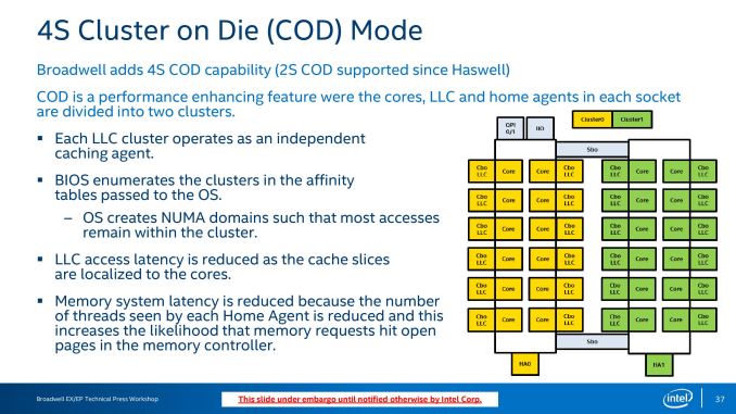
There are a couple of features for the HCC based processors that may be more relevant for the 4S systems, such as an upgraded version of Cluster on Die. Due to the configuration of the die and the dual ring design, if a core needs data in an L3 cache on the other side of the die, the latency would be higher than if it was closer to the die. To alleviate this, Haswell E5/E7 Xeons separated each die into two clusters such that each part would be seen by the BIOS as a non-unified memory domain. This allows the home agent/system agent to manage the likelihood that memory requests are aimed at data closer to the core that needs it. In Broadwell, this feature is now brought up from dual-processor systems to four-processor systems, and should reduce last level cache latency and performance for larger systems.
The new E7 v4 processors use the same socket as the previous generation, the E7 v3 processors. With a BIOS update, the new processors are a drop in with the older platform. The usual Intel partners (Supermicro, HP Enterprise, Dell, Cray) are expected to offer systems based on the new processors. We expect the new processors to cost in line with the previous generation with a typical generational increase. I believe Johan is currently in the process of testing a few parts, and I’m looking forward to the review.


26 Comments
View All Comments
Topinio - Tuesday, June 14, 2016 - link
I'm also surprised at the E7-8893 v4, wondering if the clocks are actually high -- this article is completely missing the AVX clocks (base, 1C max, and all-core max) as well as the all-core max turbo non-AVX clocks, for all these CPUs.Not just this article, of course -- the recent ones (E3-15xx v5, E5-x6xx v4) also have too. It's pretty annoying, without knowing these one can't know how many GFLOPS of potential performance are available.
Might even have missed breaking the 1 TFLOP barrier, if the all-core AVX turbo clock on the E7-8890 v4 is 2.7 GHz ...
HideOut - Tuesday, June 14, 2016 - link
This could be an instance where intel uses the lower binned chips as a sellable product so it had to keep clock speed down in order to pass validation and whatnot.Kevin G - Tuesday, June 14, 2016 - link
The presented data appears to be from ark which doesn't list AVX clock speeds. The good news is that this is less of an issue overall as apparently AVX clock only affect the particular core running AVX code, not the entire chip. While I haven't seen the max clock permitted for AVX code on these E7 v4's, if they are anything like the E5 v4's then the max clock will be the same between AVX and non-AVX code. So while the system can clock down from running AVX code, Intel's implementation this time around is much less of an issue for traditional server scenarios (HPC is another matter).Kevin G - Tuesday, June 14, 2016 - link
If you're running an embarrassing parallel job that can't fit into the memory of these E7 systems, then yes it would be more cost effective to go with more nodes and E5 chips. No way around the networking overhead in this scenario so might as well use it to your advantage to lower costs.Seekmore - Wednesday, July 6, 2016 - link
Intel's all newly launched lineup of 4800 V4 and 8800 V4 server processors from Broadwell-Ex family and their detailed info structure is similarly given in deep tech terms on http://www.comparecpus.com/en/cpus-from-intel-xeon... . But they have given a rating for different specifications which is really cool to check out. these boosters seem really promising for this roll out. let's see if they really work out as they are supposed to.Tema726 - Thursday, May 11, 2017 - link
Hello! Is there any reference on the die size? "[...] 24 physical cores at 456.12mm2 [...]" -- where is it coming from, and is there anything about the length and width of the die? Could not find it in Intel's datasheets, unfortunately