Updated: NVIDIA Announces “NVIDIA Titan X” Video Card: $1200, Available August 2nd
by Ryan Smith on July 25, 2016 11:30 AM EST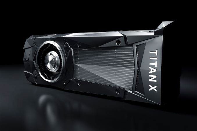
In 2014/2015, it took NVIDIA 6 months from the launch of the Maxwell 2 architecture to get GTX Titan X out the door. All things considered, that was a fast turnaround for a new architecture. However now that we’re the Pascal generation, it turns out NVIDIA is in the mood to set a speed record, and in more ways than one.
Announced this evening by Jen-Hsun Huang at an engagement at Stanford University is the NVIDIA Titan X, NVIDIA’s new flagship video card. Based on the company’s new GP102 GPU, it’s launching in less than two weeks, on August 2nd.
| NVIDIA GPU Specification Comparison | ||||||
| NVIDIA Titan X | GTX 1080 | GTX Titan X | GTX Titan | |||
| CUDA Cores | 3584 | 2560 | 3072 | 2688 | ||
| Texture Units | 224? | 160 | 192 | 224 | ||
| ROPs | 96? | 64 | 96 | 48 | ||
| Core Clock | 1417MHz | 1607MHz | 1000MHz | 837MHz | ||
| Boost Clock | 1531MHz | 1733MHz | 1075MHz | 876MHz | ||
| TFLOPs (FMA) | 11 TFLOPs | 9 TFLOPs | 6.6 TFLOPs | 4.7 TFLOPs | ||
| Memory Clock | 10Gbps GDDR5X | 10Gbps GDDR5X | 7Gbps GDDR5 | 6Gbps GDDR5 | ||
| Memory Bus Width | 384-bit | 256-bit | 384-bit | 384-bit | ||
| VRAM | 12GB | 8GB | 12GB | 6GB | ||
| FP64 | 1/32 | 1/32 | 1/32 | 1/3 | ||
| FP16 (Native) | 1/64 | 1/64 | N/A | N/A | ||
| INT8 | 4:1 | ? | ? | ? | ||
| TDP | 250W | 180W | 250W | 250W | ||
| GPU | GP102 | GP104 | GM200 | GK110 | ||
| Transistor Count | 12B | 7.2B | 8B | 7.1B | ||
| Die Size | 471mm2 | 314mm2 | 601mm2 | 551mm2 | ||
| Manufacturing Process | TSMC 16nm | TSMC 16nm | TSMC 28nm | TSMC 28nm | ||
| Launch Date | 08/02/2016 | 05/27/2016 | 03/17/2015 | 02/21/2013 | ||
| Launch Price | $1200 | MSRP: $599 Founders $699 |
$999 | $999 | ||
Let’s dive right into the numbers, shall we? The NVIDIA Titan X will be shipping with 3584 CUDA cores. Assuming that NVIDIA retains their GP104-style consumer architecture here – and there’s every reason to expect they will – then we’re looking at 28 SMs, or 40% more than GP104 and the GTX 1080.
It’s interesting to note here that 3584 CUDA cores happens to be the exact same number of CUDA cores also found in the Tesla P100 accelerator. These products are based on very different GPUs, but I bring this up because Tesla P100 did not use a fully enabled GP100 GPU; its GPU features 3840 CUDA cores in total. NVIDIA is not confirming the total number of CUDA cores in GP102 at this time, but if it’s meant to be a lightweight version of GP100, then this may not be a fully enabled card. This would also maintain the 3:2:1 ratio between GP102/104/106, as we saw with GM200/204/206.
On the clockspeed front, Titan X will be clocked at 1417MHz base and 1531MHz boost. This puts the total FP32 throughput at 11 TFLOPs (well, 10.97…), 24% higher than GTX 1080. In terms of expected performance, NVIDIA isn’t offering any comparisons to GTX 1080 at this time, but relative to the Maxwell 2 based GTX Titan X, they are talking about an up to 60% performance boost.
Feeding the beast that is GP102 is a 384-bit GDDR5X memory bus. NVIDIA will be running Titan X’s GDDR5X at the same 10Gbps as on GTX 1080, so we’re looking at a straight-up 50% increase in memory bus size and resulting memory bandwidth, bringing Titan X to 480GB/sec.

At this point in time there are a few unknowns about other specifications of the card. ROP count and texture unit count have not been disclosed (and this is something NVIDIA rarely posts on their site anyhow), but based on GP104 and GP106, I believe it’s safe to assume that we’re looking at 224 texture units and 96 ROPs respectively. To put this into numbers then, theoretical performance versus a GTX 1080 would be 24% more shading/texturing/geometry/compute performance, 50% more memory bandwidth, and 33% more ROP throughput. Or relative GTX Titan X (Maxwell 2), 56% more shading/texturing/geometry/compute performance, 43% more memory bandwidth, and 42% more ROP throughput. Of course, none of this takes into account any of Pascal’s architectural advantages such as a new delta color compression system.
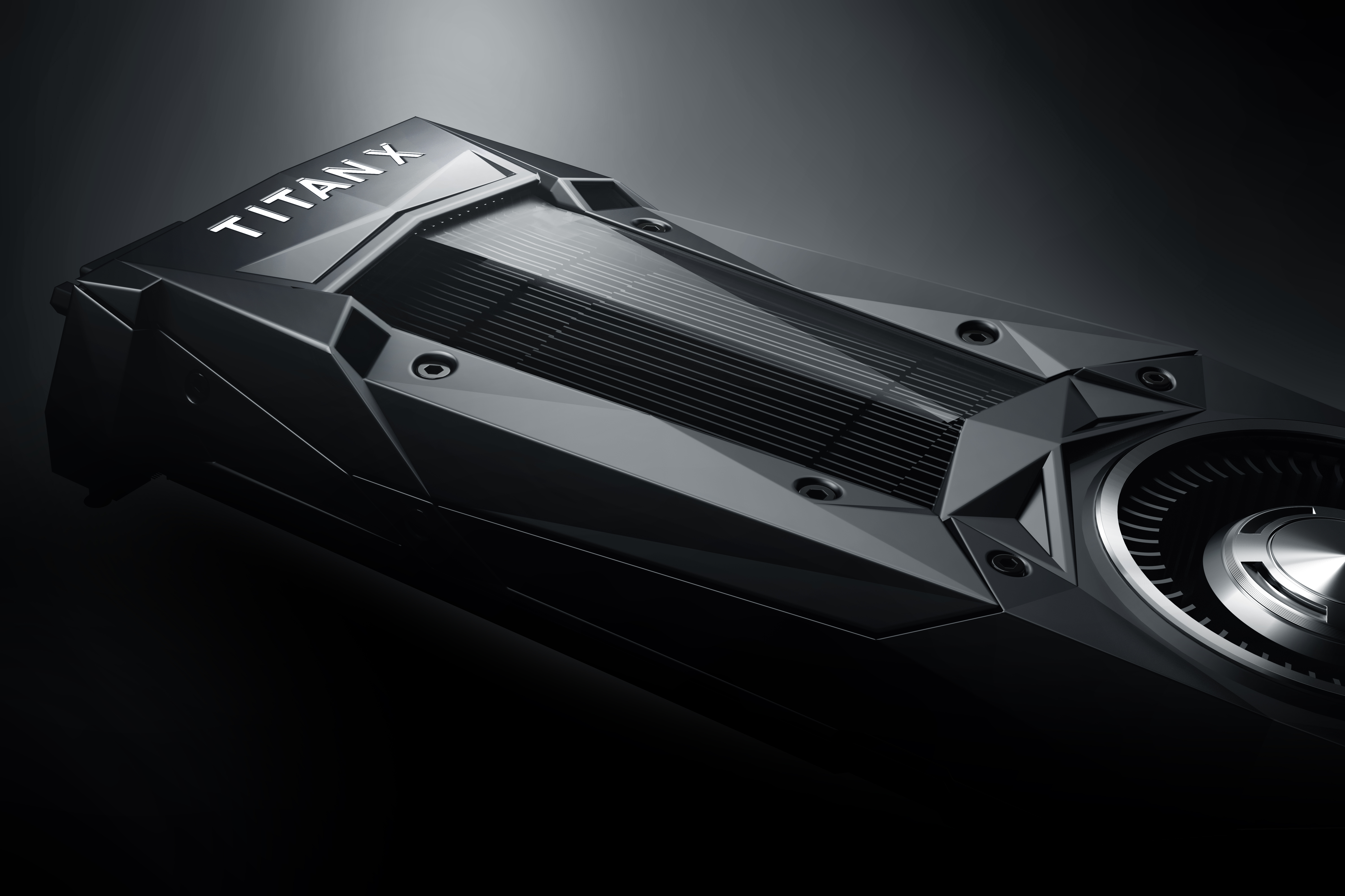
Meanwhile like the past Titans, the new Titan X is a 250W card, putting it 70W (39%) above GTX 1080. In pictures released by NVIDIA and confirmed by their spec sheet, this will be powered by the typical 8-pin + 6-pin power connector setup. And speaking of pictures, the handful of pictures released so far confirm that the card will be following NVIDIA’s previous reference design, in the new GTX 1000 series triangular style. This means we’re looking at a blower based card – now clad in black for Titan X – using a vapor chamber setup like the GTX 1080 and past Titan cards.
The TDP difference between Titan X and GTX 1080 may also explain some of rationale behind the performance estimates above. In the Maxwel 2 generation, GTX Titan X (250W) consumed 85W more than GTX 980 (165W); but for the Pascal generation, NVIDIA only gets another 70W. As power is the ultimate factor limiting performance, it stands to reason that NVIDIA can't increase performance over GTX 1080 (in the form of CUDA cores and clockspeeds) by as much as they could over GTX 980. There is always the option to go above 250W - Tesla P100 in mezzanine form goes to 300 W - but for a PCIe form factor, 250W seems to be the sweet spot for NVIDIA.
Moving on, display I/O is listed as DisplayPort 1.4, HDMI 2.0b, and DL-DVI; NVIDIA doesn’t list the number of ports (and they aren’t visible in product photos), but I’d expect that it’s 3x DP, 1x HDMI, and 1x DL-DVI, just as with the past Titan X and GTX 1080.
From a marketing standpoint, it goes without saying that NVIDIA is pitching the Titan X as their new flagship card. What is interesting however is that it’s not being classified as a GeForce card, rather it’s the amorphous “NVIDIA Titan X”, being neither Quadro, Tesla, nor GeForce. Since the first card’s introduction in 2013, the GTX Titan series has always walked a fine line as a prosumer card, balanced between a relatively cheap compute card for workstations, and an uber gaming card for gaming PCs.
That NVIDIA has removed this card from the GeForce family would seem to further cement its place as a prosumer card. On the compute front the company is separately advertising the card's 44 TOPs INT8 compute performance - INT8 being frequently used for neural network inference - which is something they haven't done before for GeForce or Titan cards. Though make no mistake: the company’s GeForce division is marketing the card and it’s listed on GeForce.com, so it is still very much a gaming card as well.
As for pricing and availability, NVIDIA’s flagships have always been expensive, and NVIDIA Titan X even more so. The card will retail for $1200, $200 more than the previous GTX Titan X (Maxwell 2), and $500 more than the NVIDIA-built GTX 1080 Founders Edition. Given the overall higher prices for the GTX 1000 series, this isn’t something that surprises me, but none the less it means buying NVIDIA’s best card just got a bit more expensive. Meanwhile for distribution, making a departure from previous generations, the card is only being sold directly by NVIDIA through their website. The company’s board partners will not be distributing it, though system builders will still be able to include it.
Overall the announcement of this new Titan card, its specifications, and its timing raises a lot of questions. Does GP102 have fast FP64/FP16 hardware, or is it purely a larger GP104, finally formalizing the long-anticipated divide between HPC and consumer GPUs? Just how much smaller is GP102 versus GP100? How has NVIDIA been able to contract their launch window by so much for the Pascal generation, launching 3 GPUs in the span of 3 months? These are all good questions I hope we’ll get an answer to, and with an August 2nd launch it looks like we won’t be waiting too long.
Update 07/25: NVIDIA has given us a few answers to the question above. We have confirmation that the FP64 and FP16 rates are identical to GP104, which is to say very slow, and primarily there for compatibility/debug purposes. With the exception of INT8 support, this is a bigger GP104 throughout.
Meanwhile we have a die size for GP102: 471mm2, which is 139mm2 smaller than GP100. Given that both (presumably) have the same number of FP32 cores, the die space savings and implications are significant. This is as best of an example as we're ever going to get on the die space cost of the HPC features limited to GP100: NVLInk, fast FP64/FP16 support, larger register files, etc. By splitting HPC and graphics/inference into two GPUs, NVIDIA can produce GP102 at what should be a significantly lower price (and higher yield), something they couldn't do until the market for compute products based on GP100 was self-sustaining.
Finally, NVIDIA has clarified the branding a bit. Despite GeForce.com labeling it "the world’s ultimate graphics card," NVIDIA this morning has stated that the primary market is FP32 and INT8 compute, not gaming. Though gaming is certainly possible - and I fully expect they'll be happy to sell you $1200 gaming cards - the tables have essentially been flipped from the past Titan cards, where they were treated as gaming first and compute second. This of course opens the door to a proper GeForce branded GP102 card later on, possibly with neutered INT8 support to enforce the market segmentation.


228 Comments
View All Comments
Yojimbo - Monday, July 25, 2016 - link
Well the update to this article confirms minimal FP16x2 support for compatibility purposes only. Someone on another message board claimed that the ultra-slow FP16 performance on the GTX 1080 is a driver bug, and NVIDIA intends FP16 to run at the same throughput and memory isage as FP32 on that card. Apparantly the FP16x2 cores must be targeted with special instructions. So it makes sense for NVIDIA to include a small number on other chips for compatability purposes even though running through the FP32 cores makes more sense on such chips.But I am surprised the GP102 doesn't use FP16x2 cores. I would have thought they'd use that GPU for an M40 successor. It seems they are pushing the P100 for learning. Baidu uses the Maxwell Titan X for training, as far as I know. The Pascal Titan X has significant FP32 performance and memory bandwidth improvement over the Maxwell Titan X. Maybe NVIDIA think that improvement is enough. Still makes me wonder about an M40 successor though.
pygosceles - Thursday, August 4, 2016 - link
Yojimbo, do you have a reference for the claim that throttled FP16 performance is a driver bug? I'd be overjoyed to learn that the GTX 1080 is not artificially crippled in that regard, especially with so many up-and-coming deep learning enthusiasts trying to advance the field with that kind of horsepower. I don't know if it could be modded to access full-speed FP16 without an alteration to the die?p1esk - Monday, July 25, 2016 - link
INT8 is implemented as dp4a operation, so it's 4 ops instead of one FP32 ops, which means 4x11=44.Yojimbo - Monday, July 25, 2016 - link
It's 8 ops. And floating point FMA is 2 ops. But it's not clear to me why we are talking about it in terms of floating point FMA. Maybe there's a reason to do so because of the hardware implementation. But regardless, it seems true that the GPU performs 8 8-bit integer operations per core per clock cycle under the right conditions. It's (8 ops)*(3584 cores)*(1.531 GHz) = 43.9 TOPS."Integer Arithmetic Instructions: dp4a
Description
Four-way byte dot product which is accumulated in 32-bit result. Operand a and b are 32-bit inputs which hold 4 byte inputs in packed form for dot product."
So if a = (a.w, a.x, a.y, a.z) and b = (b.w, b.x, b.y, b.z) then the dp4a operation computes c = a(dot)b + c = a.w*b.w + a.x*b.x + a.y*b.y + a.z*b.z + c, resulting in 4 multiplications and 4 additions for a total of 8 operations.
Yojimbo - Tuesday, July 26, 2016 - link
Sorry for my confusing notation there. The "=" after the c is meant to be an assignment and the "=" after that is meant as equality of the two expressions, excluding the assignment.tipoo - Monday, July 25, 2016 - link
I think the question marks on the int ratios for the other cards may be in this article:http://www.extremetech.com/computing/153467-amd-de...
p1esk - Monday, July 25, 2016 - link
That article is from 2013, and has no information about INT8 operations.alpha754293 - Monday, July 25, 2016 - link
I'm confused (or maybe it really is as written/posted).FP16 is 1/64 (presumably) the FP32 rate.
FP64 is 1/32.
So...FP16 is actually SLOWER than FP64? Wow. Didn't expect that.
Also, with FP32 rate being a FMA rate, I wonder what say a LINPACK FP32 speed would be (native/raw/non-FMA).
That said, it's sad (in a way) how my GTX Titan FP64 is still faster than their newest, latest, flagship card, despite the fact that its primary market IS FP32. (And I care because I think that my MATLAB code is primarily FP64 by default...)
Hmmm...interrresting.
p1esk - Monday, July 25, 2016 - link
They use separate cores for FP16, FP32, and FP64 ops in the new Titan X and in 1080. That's why performance numbers for those data types are independent. In GP100, on the other hand, each FP32 core can compute 2 FP16 ops, so that's why FP16 performance is off the charts there (unfortunately the price is off the charts as well).Harry Lloyd - Tuesday, July 26, 2016 - link
1200 $ for a 471 mm2 GPU, what a joke. There is barely any performance increase over the 1080, at double the price. This FinFET generation is pathetic so far.