Samsung at Flash Memory Summit: 64-layer V-NAND, Bigger SSDs, Z-SSD
by Billy Tallis on August 11, 2016 5:30 AM EST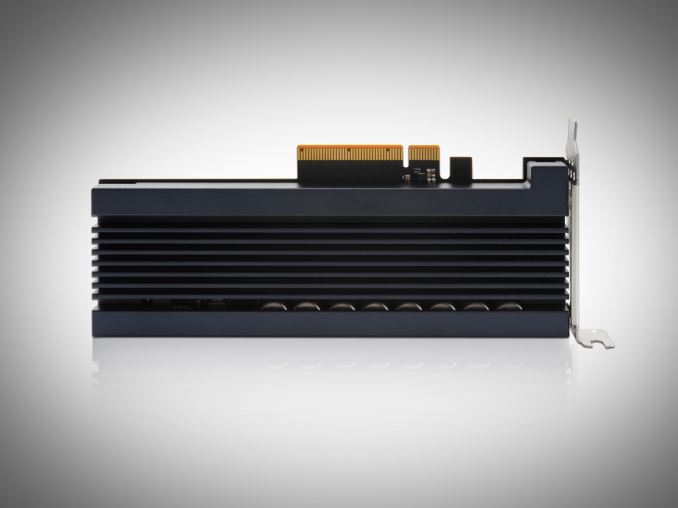
At Flash Memory Summit, Samsung announced their fourth generation of 3D NAND and several of the more obvious SSD upgrades it enables. Taking a page from Intel and Micron's strategy book, they also announced a new memory type and corresponding SSD product while saying essentially nothing about what the new memory actually is.


The fourth generation 3D NAND bumps the layer count up to 64, compared to the 48-layer design used by the third generation V-NAND that was announced last fall and has been slowly rolling out to their SSD products over the course of this year. So far Samsung has talked about a 512Gb TLC part, and at least initially the MLC parts will probably be made from the same die and thus have two thirds the capacity. (Samsung's second generation 3D NAND was initially available as 128Gb TLC or 86Gb MLC, with 128Gb MLC parts introduced later.) The new NAND also supports an increased interface speed of 800Mbps, which is key to reducing the performance penalty that comes from consolidating more flash onto fewer independent chips.
With a per-die capacity of 512Gb (64GB), Samsung can now put 1TB of TLC flash in a single package. This means most product lines will be seeing an increase in capacity at the high end of the range. Their BGA SSD products will be offering 1TB capacity even in the 11.5mm by 13mm form factor. The 16TB PM1633a SAS SSD will be eclipsed by the new 32TB PM1643. Likely to be further out, the PM1725 PCIe add-in card SSD will be succeeded by the PM1735 with a PCIe 4 x8 host interface.
Complementing the NAND update will be a new non-standard oversized M.2 form factor 32mm wide and 114mm long, compared to the typical enterprise M.2 size of 22mm by 110mm. A little extra room can go a long way, and Samsung will be using it to produce 8TB drives. These will be enterprise SSDs and Samsung showed a diagram of these enabling 256TB of flash in a 1U server. Samsung will also be producing 4TB drives in standard M.2 sizing.


In what is likely a bid to steal some thunder from 3D XPoint memory before it can ship, Samsung announced Z-NAND memory technology and a Z-SSD product based around Z-NAND and a new SSD controller. They said nothing about the operating principles of Z-NAND, but they did talk about their plans for the Z-SSD products.
Samsung Z-SSD is being marketed as addressing the performance gap between DRAM and SSDs. Samsung's slides during their keynote showed some performance comparisons against the PM963 NVMe TLC SSD and against an unnamed "PRAM based" solution. The logical point of comparison would be against 3D XPoint NVMe drives, but Samsung can't have real performance and power numbers on those when they're still under development by Intel and Micron. Thus the PRAM based solution Samsung refers to is probably one of their own earlier R&D efforts that didn't make it to market. The Z-SSD ties or comes out ahead on every benchmark Samsung showed, but NVMe NAND flash SSDs were missing from the power consumption comparison.
The slides stated that there will be a 1TB Z-SSD this year and 2TB and 4TB Z-SSDs next year, while the press release issued later states that more generally that the Z-SSD is expected to be released next year. The press release also states that Z-NAND "shares the fundamental structure of V-NAND and has a unique circuit design and controller that can maximize performance". Given that, the launch timeframe and capacities that are only a little lower than NAND flash SSDs, it seems that Z-NAND isn't drastically different from existing memory technologies and it may even be little more than SLC flash in disguise, trying for a comeback.


51 Comments
View All Comments
lilmoe - Thursday, August 11, 2016 - link
It's all about price, folks. On the consumer end, that is.ImSpartacus - Thursday, August 11, 2016 - link
Yeah, I don't see much changing there except a steady march to the bottom. All these are pro/high end products.name99 - Friday, August 12, 2016 - link
Consumer is a big space. Are Apple products consumer? Because they're a possible target for this sort of thing. (Depending on how Intel prices XPoint, however, THAT may be enterprise only for two or three years.)plopke - Thursday, August 11, 2016 - link
The more I see from Optane , QuantX , Z-SSD,... the more I wonder what the benefit is for mainstream consumer products , to expensive, coming as a cache system for consumer enthusiastic people which can buy 16/32GB DDR4 quiet cheap + very quick SSDs instead of spending money on this.But on enterprise level will be fun to watch how this all evolves.
lefty2 - Thursday, August 11, 2016 - link
I don't think anyone ever said that they have benefit for mainstream consumer products. It's mainly for enterprise and enthusiast markets.Also, Samsung only talks about performance. 3D X-point is 1000 times more longativity than normal NAND and that factor is just as important as the performance. So, what's the longativity of Z-Nand?
plopke - Thursday, August 11, 2016 - link
You are right , guess Intel is the only one who might pitch this to consumers atm.ddriver - Thursday, August 11, 2016 - link
Well, if it is indeed SLC, then it could handle 100k+ p/e cycles. That's a LOT more than MLC flash.SLC's problem was low capacity, which samsung can solve by stacking dies into a single package. I am surprised they took so long, but then again, it is not as cost effective as MLC and TLC stacking, so it makes sense they didn't do it for consumer drives, but now that the enterprise market is gearing for a transition to flash and with xpoint on the horizon, the fat profit margins of the enterprise market have made stacking SLC very viable.
bcronce - Thursday, August 11, 2016 - link
3D VAND TLC has between 10k and 70k p/e cycles, depending on if they optimize the firmware for speed or durability. I haven't heard how many cycles SLC 3D VNAND has, I assume more. The main point is modern MLC can have about the same amount of cycles as last gen SLC.ats - Thursday, August 11, 2016 - link
This is completely false on so many levels. Modern NAND and 3D NAND has significantly LESS real endurance than NAND from 5-10 years ago. What you are actually seeing are advances in redundancy and error correction codes. Those old numbers for say 50/40nm flash were RAW P/E cycles. You could hook the flash up to any interface and it would give at least those numbers of P/E cycles. What is being quoted for modern flash is not RAW P/E values but calculated P/E values assuming a certain redundancy and a certain level of error correction (generally quite complex taking microseconds to compute).frenchy_2001 - Thursday, August 11, 2016 - link
Nope.What has happened is that 3D NAND took multiple steps back in XY lithography and then went 3D (up) and stacked layers.
So, recent 3D NAND are back on the 40nm process (instead of 16nm process for planar NAND). This gives them *MUCH* bigger cells, thicker walls and as such, better endurance. Process improvements helped too.
Basically, 3D NAND is back to RAW p/e cycles superior to what we had in the past, just due to cell size. On top of that, they now have better error correction and better wear leveling and controllers. This is why even TLC in 3D NAND has decent endurance.