HiSilicon Kirin 960: A Closer Look at Performance and Power
by Matt Humrick on March 14, 2017 7:00 AM EST- Posted in
- Smartphones
- Mobile
- SoCs
- HiSilicon
- Cortex A73
- Kirin 960
HiSilicon’s Kirin 950 proved to be a breakout product for the Huawei subsidiary, ultimately finding a home in many of Huawei’s flagship phones, including the Mate 8, P9, P9 Plus, and Honor 8. Its big.LITTLE combination of four A72 and four A53 CPU cores manufactured on TSMC’s 16nm FF+ FinFET process delivered excellent performance and efficiency. Somewhat surprisingly, it turned out to be one of the best, if not the best, implementation of ARM’s IP we’ve seen.
Because of the 950’s success, we were eager to see what improvements the Kirin 960 could offer. In our review of the Huawei Mate 9, the first device to use the new SoC, we saw gains in most of our performance and battery life tests relative to the Mate 8 and its Kirin 950 SoC. Now it’s time to dive a little deeper and answer some of our remaining questions: How does IPC compare between the A73, A72, and other CPU cores? How is memory performance impacted by the A73’s microarchitecture changes? Does CPU efficiency improve? How much more power do the extra GPU cores consume?
| HiSilicon High-End Kirin SoC Lineup | |||
| SoC | Kirin 960 | Kirin 955 | Kirin 950 |
| CPU | 4x Cortex-A73 @ 2.36GHz 4x Cortex-A53 @ 1.84GHz |
4x Cortex-A72 @ 2.52GHz 4x Cortex-A53 @ 1.81GHz |
4x Cortex-A72 @ 2.30GHz 4x Cortex-A53 @ 1.81GHz |
| GPU | ARM Mali-G71MP8 1037MHz |
ARM Mali-T880MP4 900MHz |
|
| Memory | 2x 32-bit LPDDR4 @ 1866MHz 29.9GB/s |
2x 32-bit LPDDR3 @ 933MHz (14.9GB/s) or 2x 32-bit LPDDR4 @ 1333MHz (21.3GB/s) (hybrid controller) |
|
| Interconnect | ARM CCI-550 | ARM CCI-400 | |
| Storage | UFS 2.1 | eMMC 5.0 | |
| ISP/Camera | Dual 14-bit ISP (Improved) |
Dual 14-bit ISP 940MP/s |
|
| Encode/Decode | 2160p30 HEVC & H.264 Decode & Encode 2160p60 HEVC Decode |
1080p H.264 Decode & Encode 2160p30 HEVC Decode |
|
| Integrated Modem | Kirin 960 Integrated LTE (Category 12/13) DL = 600Mbps 4x20MHz CA, 64-QAM UL = 150Mbps 2x20MHz CA, 64-QAM |
Balong Integrated LTE (Category 6) DL = 300Mbps 2x20MHz CA, 64-QAM UL = 50Mbps 1x20MHz CA, 16-QAM |
|
| Sensor Hub | i6 | i5 | |
| Mfc. Process | TSMC 16nm FFC | TSMC 16nm FF+ | |
The Kirin 960 is the first SoC to use ARM’s latest A73 CPU cores, which seems fitting considering the Kirin 950 was the first to use ARM’s A72. Its CPU core frequencies see a negligible increase relative to the Kirin 950: 1.81GHz to 1.84GHz for the four A53s and 2.30GHz to 2.36GHz for the four A73s. Setting the peak operating point for the A73 cores lower than the 2.52GHz used by Kirin 955’s A72 cores, and lower still than the 2.8GHz that ARM targets for 16nm, is an interesting and deliberate choice by HiSilicon to limit the CPU’s power envelope, allowing the bigger GPU to take a larger chunk.
We’ve already discussed the A73’s microarchitecture in depth, so I’ll just summarize a few of the highlights. For starters, the A73 stems from the A17 and does not belong to the A15/A57/A72 Austin family tree. This means the differences between the A72 and A73 are more substantial than the small change in product numbering would suggest, particularly in the CPU’s front end.
The biggest difference is a reduction in decoder width, which is now 2-wide instead of 3-wide like the A72. This sounds like a downgrade on paper; however, there’s likely some workloads where the A72’s instruction fetch block fails to consistently saturate the decoder, so the actual performance impact of the A73’s narrower decode stage may not be that severe.
In many cases, instruction dispatch throughput should actually improve relative to the A72. The A73’s shorter pipeline reduces front-end latency, including 1-2 fewer cycles for the decoder, which can decode most instructions in a single cycle, and 1 less cycle for the fetch stage. The L1 instruction cache doubles in size and is optimized for better throughput, and changes to the instruction fetch block reduce instruction bubbles. ARM also says the A73 includes a new, more accurate branch predictor, with a larger BTAC (Branch Target Address Cache) structure and a new 64-entry “micro-BTAC” for accelerating branch prediction.
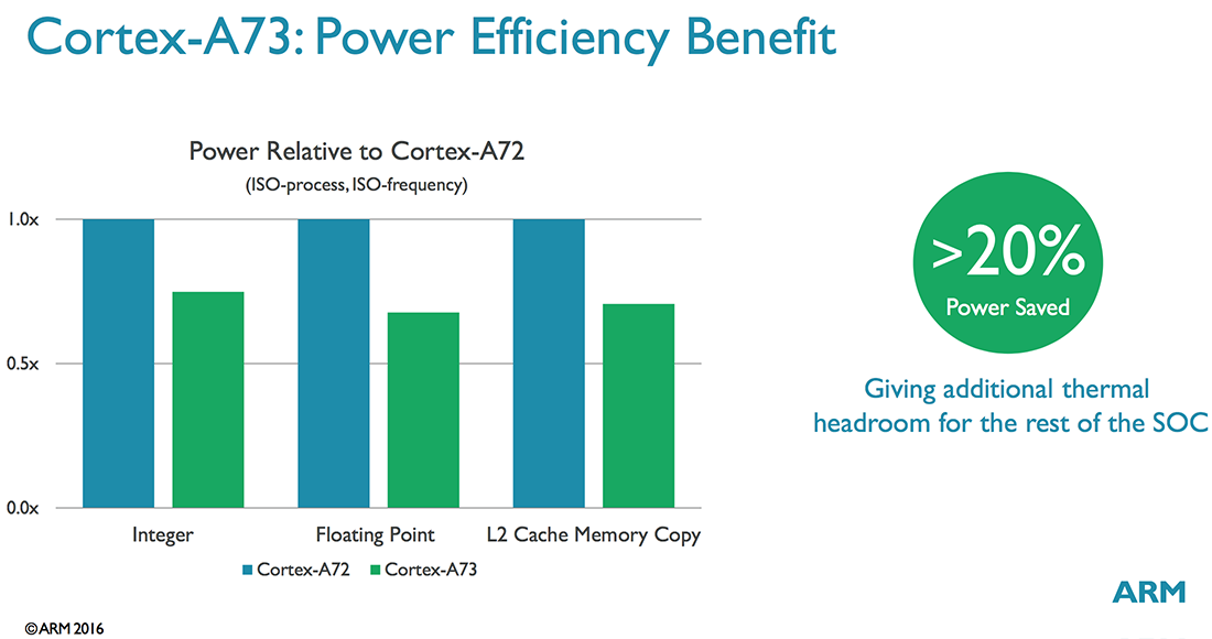
There are several other changes to the front end too, not to mention further along the pipeline, but it should be obvious by now that the A73 is a very different beast than the A72, grown from a different design philosophy. While the Austin family (A72) targeted industrial and low-power server applications in addition to mobile, the A73 focuses specifically on mobile, where power and area become an even higher priority. ARM says the A73 consumes 20%-30% less power than the A72 (same process, same frequency) and is up to 25% smaller (same process, same performance targets).
When it comes to Kirin 960’s GPU, however, HiSilicon is clearly chasing performance instead of efficiency. With its previous SoCs, the Kirin 950/955 in particular, HiSilicon was criticized for using four-core Mali configurations while Samsung packed in eight or twelve Mali cores in its Exynos SoCs and Qualcomm squeezed more ALU resources into its Adreno GPUs. This was not entirely justified, though, because the Kirin 950’s Mali-T880MP4 GPU was capable of playing nearly any game available at acceptable frame rates and the performance difference between the Mate 8 (Kirin 950), Samsung Galaxy S7 edge (Snapdragon 820), and Galaxy S7 (Exynos 8890) after reaching thermal equilibrium is minimal.
Whether in response to this criticism or to enable future use cases such as VR/AR, HiSilicon has significantly increased the Kirin 960’s peak GPU performance. Not only is it the first to use ARM’s latest Mali-G71 GPU, but it doubles core count to eight and boosts the peak frequency to 1037MHz, 15% higher than the 950’s smaller GPU.
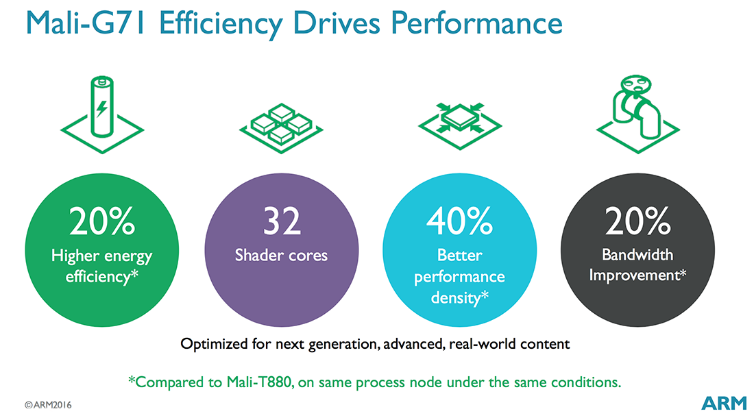
The Mali-G71 uses ARM’s new Bifrost microarchitecture, which moves from an SIMD ISA that relied on Instruction Level Parallelism (ILP) to a scalar ISA designed to take advantage of Thread Level Parallelism (TLP) like modern desktop GPU architectures from Nvidia and AMD. I’m not going to explain the difference in depth here, but basically this change allows better utilization of the shader cores, increasing throughput and performance. ARM’s previous Midgard microarchitecture needed to extract 4 instructions from a single thread and execute them concurrently to achieve full utilization of a single shader core, which is not easy to do consistently. In contrast, Bifrost can group 4 separate threads together on a shader core and execute a single instruction from each one, which is more inline with modern graphics and compute workloads.
Now that we have a better understanding for Kirin 960’s design goals—better efficiency for the CPU and higher peak performance for the GPU—and a summary of the hardware changes HiSilicon made to achieve them, we’re ready to see how the performance and power consumption of the Kirin 960 compares to the 950/955 and other recent SoCs.


86 Comments
View All Comments
BedfordTim - Tuesday, March 14, 2017 - link
I suspect it comes down to cost and usage. The iPhone cores are roughly four times the size of an A73.name99 - Tuesday, March 14, 2017 - link
True. But the iPhone cores are still small ENOUGH. The main CPU complex on an A10 (two big cores, two small cores, and L2, is maybe 15 mm^2.ARM STILL seems to be optimizing for core area, and then spending that same core area anyway in octacores and decacores. It makes no sense to me.
Obviously part of it is that Apple must be throwing a huge number of engineers at the problem. But that's not enough; there has to be some truly incredible project management involved to keep all those different teams in sync, and I don't think anyone has a clue how they have done that.
They certainly don't seem to be suffering from any sort of "mythical man-month" Fred Brooks problems so far...
My personal suspicion is that, by luck or by hiring the best senior engineer in the world, they STARTED OFF at a place that is pretty much optimal for the trajectory they wanted.
They designed a good 3-wide core, then (as far as anyone can tell) converted that to a 6-wide core by clustering and (this is IMPORTANT) not worrying about all the naysayers who said that a very wide core could not be clocked very high.
Once they had the basic 6-wide core in place, they've had a superb platform on top of which different engineers can figure out improved sub-systems and just slot them in when ready. So we had the FP pipeline redesigned for lower latency, we had an extra NEON functional unit added, we've doubtless had constant improvements to branch prediction, I-fetching, pre-fetching, cache placement and replacement; and so on --- but these are all (more or less) "easy" to optimize given a good foundation on which to build.
I suspect, also, that unlike some in the industry, they have been extremely open to new ideas from academia, so that there's an implementation turnaround time of maybe two years or so from encountering a good idea (say a new design for a cluster predictor) through simulating it to validate its value, to implementing it.
I'm guessing that management (again unlike most companies) is willing to entertain a constant stream of ideas (from engineers, from reading the literature, from talking to academics) and to ACCEPT and NOT COMPLAIN about the cost of writing the simulations, in the full understanding that only 5 or 10% of simulated ideas are worth emulating. My guess is that they've managed to increase frequency rapidly (in spite of the 6-wide width) by implementing a constant stream of the various ideas that have been published (and generally mocked or ignored by the industry) for ways to scale things like load-store queues, issue, and rename --- the standard frequency/power pain-points in OoO design.
Meanwhile ARM seems to suffer from terminal effort-wasting. Apple has a great design, which they have been improving every year. ARM's response, meanwhile, has been to hop like a jack rabbit from A57 to A72 to A73, with no obvious conceptual progression. If each design spends time revising basics like the decoder and the optimal pipeline width, there's little time left to perform the huge number of experiments that I think Apple perform to keep honing the branch predictors, the instruction fusion, the pre-fetchers, and so on.
It reminds me of a piece of under-appreciated software, namely Mathematica, which started off with a ridiculously good foundation and horrible performance. But because the foundation was so good, every release had to waste very little time re-inventing the wheel, it could just keep adding and adding, until the result is just unbelievable.
Meteor2 - Wednesday, March 15, 2017 - link
Didn't Jim Keller have something to do with their current architecture?And yes, Apple seems to have excellent project management. Really, they have every stage of every process nailed. They're not the biggest company in the world by accident.
Meteor2 - Wednesday, March 15, 2017 - link
Also don't forget that (like Intel) ARM has multiple design teams. A72 and A73 are from separate teams; from that perspective, ARM's design progression does make sense. The original A73 'deepdive' by Andrei explained it very well.name99 - Wednesday, March 15, 2017 - link
This is a facet of what I said about project management.The issue is not WHY there are separate CPU design teams --- no-one outside the companies cares about the political compromises that landed up at that point.
The issue is --- are separate design teams and restarting each design from scratch a good fit to the modern CPU world?
It seems to me that the answer has been empirically answered as no, and that every company that follows this policy (which seem to include IBM, don't know about QC or the GPU design teams) really ought to rethink. We don't recreate compilers, or browsers, or OS's every few years from scratch, but we seem to have taken it for granted that doing so for CPUs made sense.
I'm not sure this hypothesis explains everything --- no-one outside Apple (and few inside) have the knowledge necessary to answer the question. But I do wonder if the biggest part of Apple's success came from their being a SW company, and thus looking at CPU design as a question of CONSTANTLY IMPROVING a good base, rather than as a question of re-inventing the wheel every few years the way the competition has always done things.
Meteor2 - Wednesday, March 15, 2017 - link
Part of having separate teams is to engender competition; another is to hedge bets and allow risk-taking. Core replacing Netburst is the standard example, I suppose. I'm sure there are others but they aren't coming to mind at the moment... Does replacing Windows CE with Windows 10 count?Meteor2 - Wednesday, March 15, 2017 - link
Methinks it's more to do with Safari having some serious optimisations for browser benchmarks baked in deep.I'd like to see the A10 subjected to GB4 and SpecInt.
name99 - Wednesday, March 15, 2017 - link
The A10 GeekBench numbers are hardly secret. Believe me, they won't make you happy.SPEC numbers, yeah, we're still waiting on those...
name99 - Wednesday, March 15, 2017 - link
Here's an example:https://browser.primatelabs.com/v4/cpu/959859
Summary:
Single-Core Score 3515
Crypto Score 2425
Integer Score 3876
Floating Point Score 3365
Memory Score 3199
The even briefer summary is that basically every sub-benchmark has A10 at 1.5x to 2x the Kirin 960 score. FP is even more brutal with some scores at 3x, and SGEMM at ~4.5x.
(And that's the A10... The A10X will likely be out within a month, likely fabbed on TSMC 10nm, likely an additional ~50% faster...)
Meteor2 - Wednesday, March 15, 2017 - link
Thanks. Would love to see those numbers in Anandtech charts, and normalised for power.