MediaTek Announces Helio X30 Availability: 10 CPU Cores On 10nm
by Matt Humrick on February 27, 2017 8:35 PM EST- Posted in
- Smartphones
- Mobile
- Trade Shows
- SoCs
- MediaTek
- Helio
- MWC_2017
- Helio X30
MediaTek first unveiled the Helio X30—its next-generation high-end SoC—last fall, but today at Mobile World Congress the Taiwanese company announced its commercial availability. The Helio X30 is entering mass production and should make its debut inside a mobile device sometime in Q2 2017.
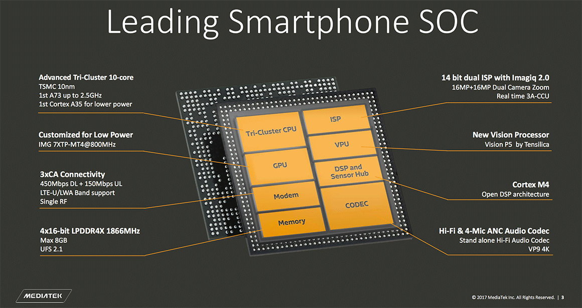
The Helio X30, like the Helio X20 family before it, incorporates 10 CPU cores arranged in a Max.Mid.Min tri-cluster configuration. Two of ARM’s latest A73 CPU cores replace the two A72s in the Max cluster, which should improve performance and reduce power consumption. The Mid cluster still uses 4 A53 cores, but they receive a 10% frequency boost relative to the top-of-the-line Helio X27. In the X30’s Min cluster we find the first implementation of ARM’s most-efficient A-series core. The A35 consumes 32% less power than the A53 it replaces (same process/frequency), while delivering 80%-100% of the performance, according to ARM. With a higher peak frequency of 1.9GHz, the X30’s A35 cores should deliver about the same or better performance than the X20’s A53 cores and still consume less power.
| MediaTek Helio X20 vs. Helio X30 | ||
| SoC | MediaTek Helio X20 |
MediaTek Helio X30 |
| CPU | 2x Cortex-A72 @2.1GHz 4x Cortex-A53 @1.85GHz 4x Cortex-A53 @1.4GHz |
2x Cortex-A73 @2.5GHz 4x Cortex-A53 @2.2GHz 4x Cortex-A35 @1.9GHz |
| GPU | ARM Mali-T880MP4 @780MHz |
PowerVR 7XTP-MT4 @800MHz |
| Memory Controller |
2x 32-bit @ 933MHz LPDDR3 14.9GB/s b/w |
4x 16-bit @ 1866MHz LPDDR4x 29.9GB/s b/w |
| Video Encode/ Decode |
encode: 2160p30 H.264 / HEVC w/HDR decode: 2160p30 10-bit H.264 / HEVC / VP9 |
encode: 2160p30 H.264 / HEVC w/HDR / VP9 decode: 2160p30 10-bit H.264 / HEVC / VP9 |
| Camera/ISP | Dual ISP 32MP @ 24fps (single camera) or 13MP + 13MP @ 30fps (dual camera) |
Dual 14-bit ISP 28MP @ 30fps (single camera) or 16MP + 16MP (dual camera) |
| Integrated Modem |
LTE Category 6 DL = 300Mbps 2x20MHz CA, 64-QAM UL = 50Mbps 1x20MHz CA, 16-QAM FDD-LTE / TD-LTE / TD-SCDMA / WCDMA / CDMA / GSM |
LTE Category 10 DL = 450Mbps 3x20MHz CA, 64-QAM UL = 150Mbps 2x20MHz CA, 64-QAM FDD-LTE / TD-LTE / TD-SCDMA / WCDMA / CDMA / GSM |
| Mfc. Process | TSMC 20SoC (planar) | TSMC 10nm FinFET |
The Helio X30 will also be the first SoC to use TSMC’s 10nm process, which will offer significant power savings relative to TSMC’s 20nm planar process that the Helio X20 family uses. According to MediaTek, the X30 consumes 50% less power than the X20 when running an unspecified CPU workload and 60% less power when running GFXBench T-Rex. These power savings will increase battery life and improve sustained performance with less thermal throttling.
Alongside the Helio X30, MediaTek is launching CorePilot 4.0, which manages CPU frequency and task scheduling. Optimized for its unique tri-cluster CPU configuration, CorePilot keeps track of the SoC’s power budget by monitoring temperature, and the global task scheduler component is responsible for migrating tasks between clusters based on workload and user experience parameters, such as frames per second. It also adjusts CPU frequency using Fast DVFS technology that increases sampling rate, allowing for faster voltage/frequency adjustments that better follow changes in workload. The overall goal of CorePilot 4.0 is to achieve the best possible performance at the lowest power levels.
In a short presentation at its MWC booth Monday, Executive Vice President & Co-COO Jeffrey Ju stated that MediaTek expects only a limited number of phones to use the Helio X30, perhaps less than ten. He also mentioned that a low yield rate for TSMC’s 10nm process has delayed the X30’s availability. The X30 sounds compelling on paper, so it will be interesting to see how many design wins it can actually achieve.


57 Comments
View All Comments
andrewaggb - Tuesday, February 28, 2017 - link
I wish they'd give some real-world examples comparing their design to some competitors. Logically I get it, A35's for idle/low load (low power, low clocks), A53's (mid power, mid clocks), and A73's for high performance.But there are only 2 A73's and 4 A53's and 4 A35's. You'd think you should have 4 A73's and are there scenarios where 4 A53's may match or exceed? Can you run the A73's with the A53's?
Why not just 4 A35's and 4 A73's? What is the cluster switching penalty? Are cache lines and everything the same or will some software need to be recompiled or be aware of these changes.
Anyways it's interesting and sounds pretty good, just wish we had more information. It's also interesting because intel and AMD haven't used this approach (atom cores + core) or (jaguar + bulldozer) and instead have favored dynamically adjusting clock speeds across a wide range.
Matt Humrick - Tuesday, February 28, 2017 - link
It's a tradeoff between performance and power/area. The cost of adding additional big cores is not negligible. All 3 clusters (or 2 in conventional big.little) can be online at the same time. The latency penalty for hotplugging cores and migrating threads between clusters is more than offset by the additional performance of the big cores (or lower power going the other way). The use of a high-bandwidth, cache-coherent (at the hardware level) interconnect reduces the migration penalty.abufrejoval - Tuesday, February 28, 2017 - link
I keep hearing that at least the small cores are really tiny in terms of surface area. I remember overall 15% for all CPU cores, BIG and little on the SoC and that was a couple of generations back. Within those 15% the big A73 core may relatively large in terms of surface area, not only for the far more complex OoO logic etc. but because they require big caches for effective work. Then adding one, two or four small cores may add single digit surface percentage, because last level caches remain shared, primary caches are tiny and less needed at the slow speeds but most importantly allow more GPU block connections to keep those busy for "perceived" speed on scrolls, video etc., whilst the big cores are sleeping.In addition those extra CPU cores won't cost much in terms of ARM licensing fees, because the biggest charge is on the number of the BIG cores, the smaller ones seem to be thrown in to the bundle.
Silicon real-estate and licensing fee economicy should perhaps get more editorial space to lessen these confusions, but few vendors seem willing to talk about them.
serendip - Wednesday, March 1, 2017 - link
What the mobile segment really needs isn't a bunch of barely differentiated CPU cores, it needs a freaking ton of small GPU cores that support programming a la CUDA or OpenCL. I'm already happy with a 4x little and 2x big core setup. Having access to hundreds of programmable simple cores would be great for custom image processing, neural networks, sound processing etc. as long as those cores are easily accessible. DSPs hidden behind proprietary blobs like Qualcomm's Hexagon don't count.Meteor2 - Tuesday, March 14, 2017 - link
Tegra X1.extide - Sunday, May 7, 2017 - link
FWIW, to give an example a single A72/73 core is bigger than an entire quad core cluster of A35/53 cores. It's cheaper (in terms of transistor budget or die size) to add a whole cluster of A53's than to add even a single extra A72/73, so to add two more is quite a bit different. I bet thats a large reason MTK is pushing these cores, 10>8 = great for marketing and less die space is great for the bottom line...nandnandnand - Wednesday, December 1, 2021 - link
I'm from the future! Intel and AMD are using this approach!