Samsung’s Multi-Billion Fab in Pyeongtaek Starts Production of 64-Layer V-NAND
by Anton Shilov on July 6, 2017 11:30 AM EST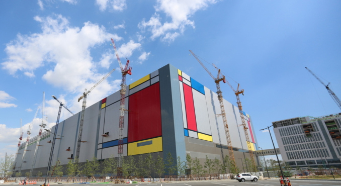
Samsung on Tuesday announced that it had started mass production of 64-layer V-NAND memory in its newly build fab in Pyeongtaek, South Korea, and the first batch had already been shipped to one of the company’s customers. The new fab was intended to focus on DRAM manufacturing, but in the light of NAND flash shortage the company adjusted its plans at some point and now the plant produces V-NAND.
Samsung’s semiconductor manufacturing facility in Pyeongtaek will be the largest and one of the most expensive fabs in the world once it ramps up its production to full capacity. Samsung announced plans to build it in October, 2014, and then started construction in April, 2015. Initially, Samsung announced plans to invest ₩15.6 trillion (around $13.5 billion at the current exchange rate) in the facility, but over the past couple of years, it announced further expansion plans for the fab. As a result, investments in the Pyeongtaek facility will total ₩30 trillion ($26.1 billion) by 2021, making the complex the most expensive semiconductor manufacturing facility ever.
According to some reports, Samsung initially planned to produce DRAM in its new fab, but given its size and scale, it was doubtful that the plant would be used only for DRAM. As it appears, Samsung decided to produce fourth-generation 3D V-NAND flash memory in its Pyeongtaek facility first, possibly because there is growing demand for NAND by Samsung’s own divisions, including Samsung Mobile. It remains to be seen when the fab in Pyeongtaek starts to manufacture DRAM ICs, which are also in short supply nowadays. Keep in mind that 3D NAND and DRAM components are produced using completely different process technologies and the former requires some additional equipment. Therefore, Samsung and other memory makers cannot switch from NAND to DRAM and vice versa without some level of equipment adjustment and reconfiguration of fab space.
At present, Samsung does not talk about the number of wafer starts at the Pyeongtaek fab because it is not operating at full capacity. That said, the plant is not going to have a substantial impact on global NAND supply in the coming weeks or months. Once fully ramped several quarters down the road, the Pyeongtaek facility will have a significant impact on both NAND and DRAM industries, as it will increase the output of both types of memory (assuming that it will be used for DRAM in the coming quarters).
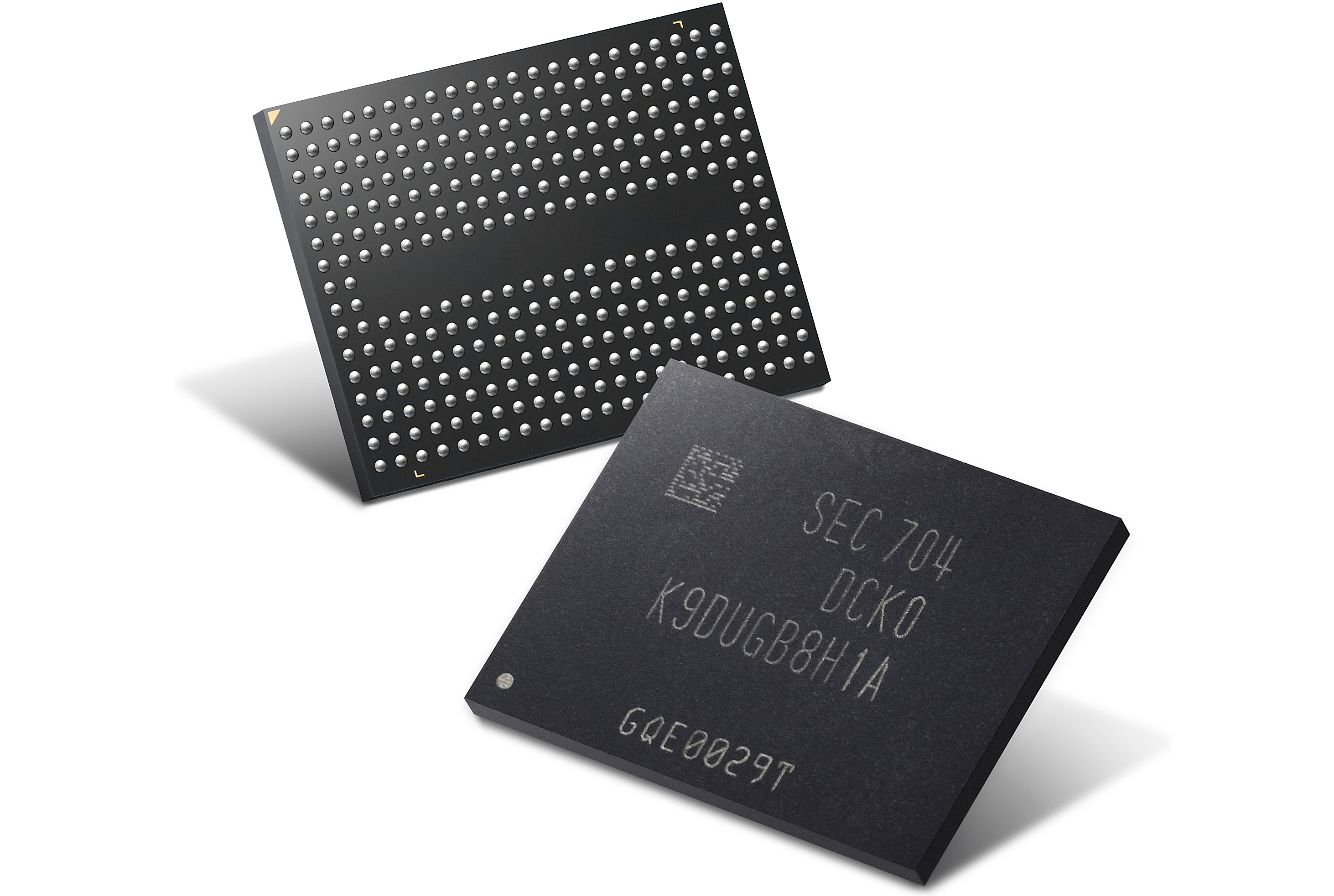
Samsung does not disclose what kind of flash memory chips it produces in terms of capacity and performance, but says that they rely on its 64-layer V-NAND design. So far, the company officially has announced only two 64-layer V-NAND ICs. First is the 512 Gb 3D TLC NAND chip with an 800 MT/s interface data rate that the company demonstrated at the Flash Memory Summit 2016. Second, the 256 Gb 3D TLC NAND IC with a 1000 MT/s interface data rate, the company launched earlier this year and began to produce in high volume in June (presumably at another facility).
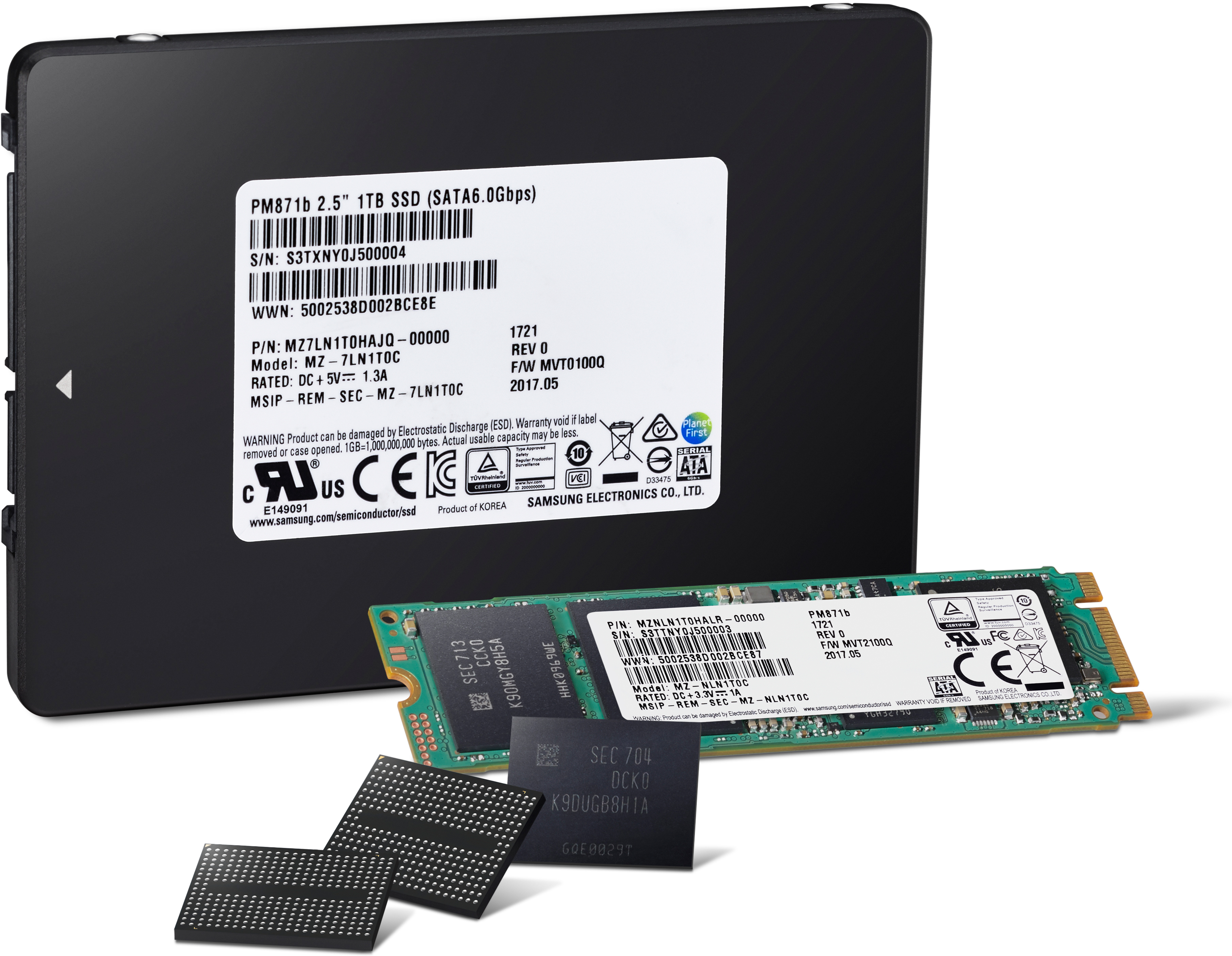
Manufacturing of 64-layer 256 Gb chips in at least two facilities indicates that Samsung is ramping up volume production of its fourth-generation V-NAND chips and therefore it is logical to expect new products based on such ICs (e.g., SSDs, memory cards, etc.) to hit the market in the coming months. Among the more interesting products will be higher-end SSDs based on 256 Gb V-NAND chips featuring a faster interface, but it remains to be seen what kind of real-world performance advantages they are going to bring given the bandwidth limitations of PCIe 3.0 x4 bus (used for NVMe M.2 drives), or for smaller capacities. So far, Samsung has only introduced the OEM-oriented PM871b SATA SSDs in 2.5" and M.2 form-factors based on its fourth-gen V-NAND memory.
Related Reading
- Samsung at Flash Memory Summit: 64-layer V-NAND, Bigger SSDs, Z-SSD
- Samsung Announces 960 PRO And 960 EVO M.2 PCIe SSDs (Updated)
- The Samsung 960 Pro (2TB) SSD Review
- The Samsung 960 EVO (1TB) Review
- SK Hynix Launches 72-Layer 256 Gb 3D TLC NAND with Increased Performance
- Western Digital Announce BiCS4 3D NAND: 96 Layers, TLC & QLC, Up to 1 Tb per Chip
- Toshiba's 768Gb 3D QLC NAND Flash Memory: Matching TLC at 1000 P/E Cycles?
Source: Samsung


16 Comments
View All Comments
Space Jam - Thursday, July 6, 2017 - link
Prices should lower with this going forward.Personally, I imagine the demand for NAND is very elastic and thus prices won't drop considerably.
EasyListening - Wednesday, July 12, 2017 - link
Ditto. Sounds like a facility big enough to handle many jobs running at full tilt. It's like, ok, homework's done. Now to scale this mofo and cash in on some economies of scale."Samsung...doesn't really FAB for other people." Qualcomm Snapdragon 835 is fabbed at Samsung on their 10nm. According to this article, http://www.gsmarena.com/qualcomm_is_going_with_tsm... , Qualcomm was 40% of Samsung's foundry sales.
Dr. Lisa Su, AMD CEO, did her PhD thesis on a finfet manufacturing technique known as Silicon-on-Insulator, or SOI. Turns out that Samsung studied SOI and went with that approach rather than do what Intel was doing with a different approach called Bulk Silicon. Intel ran into serious problems, causing major delays, to the point that Samsung, which started getting into 14nm finfet a while after Intel started on it, nearly beat Intel to market with their competing process.
Must have been interesting for Samsung to go over to AMD/GloFo with their latest research on SOI and showing Su what they had come up with. Su is one of the most respected research engineers in the semiconductor industry. Her accomplishments are quite impressive to anyone who likes to nerd out about that sort of stuff.
Long story short, Samsung outmaneuvers Intel by developing a 14nm process that shrinks relatively easily to 7nm while everyone else, Intel included, putzes around at 10nm. You know what else is shrinking? Intel's margins. Intel's CEO is looking more and more out of his depth these days.
Eric Klien - Wednesday, July 12, 2017 - link
"Samsung...doesn't really FAB for other people." They fab for many companies including Nvidia. They make the 1030, 1050, and 1050 Ti for Nvidia.prateekprakash - Thursday, July 6, 2017 - link
Larger capacity please... For archival purposes... 8TB 2.5" and 16TB 2.5" would be great...Elsote - Thursday, July 13, 2017 - link
Could this fab be used to build HMB ram?