Intel Displays 10nm Wafer, Commits to 10nm ‘Falcon Mesa’ FPGAs
by Ian Cutress on September 19, 2017 8:30 AM EST
On the back of Intel’s Technology and Manufacturing Day in March, the company presented another iteration of the information at an equivalent event in Beijing this week. Most of the content was fairly similar to the previous TMD, with a few further insights into how some of the technology is progressing. High up on that list would be how Intel is coming along with its own 10nm process, as well as several plans regarding the 10nm product portfolio.
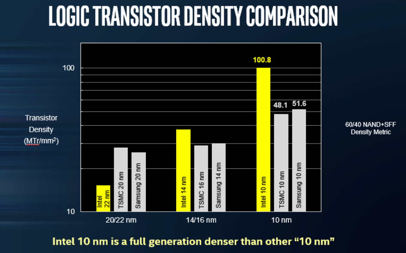
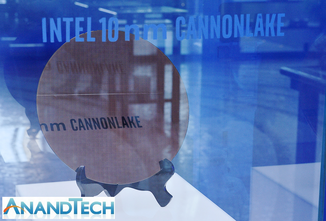
The headline here was ‘we have a wafer’, as shown in the image above. Intel disclosed that this wafer was from a production run of a 10nm test chip containing ARM Cortex A75 cores, implemented with ‘industry standard design flows’, and was built to target a performance level in excess of 3 GHz. Both TSMC and Samsung are shipping their versions of their ‘10nm’ processes, however Intel reiterated the claim that their technology uses tighter transistors and metal pitches for almost double the density of other competing 10nm technologies. While chips such as the Huawei Kirin 970 from TSMC’s 10nm are in the region of 55 million transistors per mm2, Intel is quoting over 100 million per mm2 with their 10nm (and using a new transistor counting methodology).
Intel quoted a 25% better performance and 45% lower power than 14nm, though failed to declare if that was 14nm, 14+, or 14++. Intel also stated that the optimized version of 10nm, 10++, will boost performance 15% or reduce power by 30% from 10nm. Intel’s Custom Foundry business, which will start on 10nm, is offering customers two design platforms on the new technology: 10GP (general purpose) and 10HPM (high performance mobile), with validated IP portfolios to include ARM libraries and POP kits and turnkey services. Intel has yet to announce a major partner in its custom foundry business, and other media outlets are reporting that some major partners that had signed up are now looking elsewhere.
Earlier this year Intel stated that its own first 10nm products would be aiming at the data center first (it has since been clarified that Intel was discussing 10nm++). At the time it was a little confusing, given Intel’s delayed cadence with typical data center products. However, since Intel acquired Altera, it seems appropriate that FPGAs would be the perfect fit here. Large-scale FPGAs, due to their regular repeating units, can take advantage of the smaller manufacturing process and still return reasonable yields by disabling individual gate arrays with defects and appropriate binning. Intel’s next generation of FPGAs will use 10nm, and they will go by the codename “Falcon Mesa”.
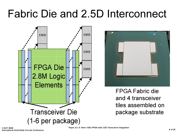
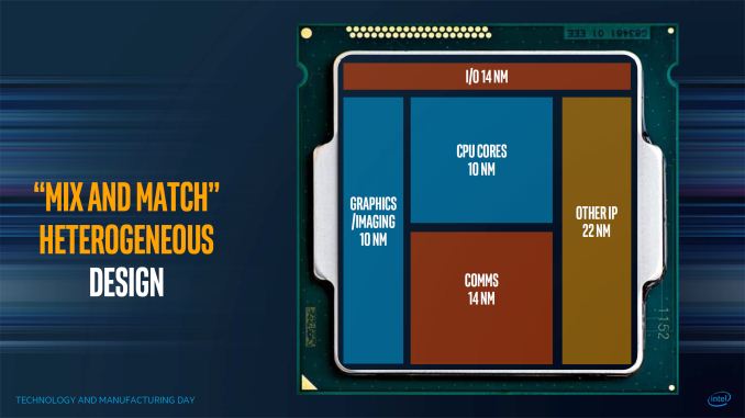
Falcon Mesa will encompass multiple technologies, most noticeably Intel’s second generation of their Embedded Multi-Die Interconnect Bridge (EMIB) packaging. This technology embeds the package with additional silicon substrates, providing a connection between separate active silicon parts much faster than standard packaging methods and much cheaper than using full-blown interposers. The result is a monolithic FPGA in the package, surrounded by memory or IP blocks, perhaps created at a different process node, but all using high-bandwidth EMIB for communication. On a similar theme, Falcon Mesa will also include support for next-generation HBM.
Possibilities with EMIB
Among the IP blocks that can be embedded via EMIB with the new FPGAs, Intel lists both 112 Gbps serial transceiver links as well as PCIe 4.0 x16 connectivity, with support for data rates up to 16 GT/s per lane for future data center connectivity. This was discussed at the recent Hot Chips conference, in a talk I’d like to get some time to expand in a written piece.
No additional information was released regarding 10nm products for consumer devices.
Related Reading
- Intel Officially Reveals Post-8th Gen Core Code Name: Ice Lake, Built on 10nm+
- Hot Chips: Intel EMIB and 14nm Stratix 10 FPGA Live Blog
- CES 2017: Intel Press Event Live Blog
- Samsung and TSMC Roadmaps: 8 and 6 nm Added, Looking at 22ULP and 12FFC


Additional: 1:00pm September 19th
After doing some digging, we have come across several shots of the wafer up close.
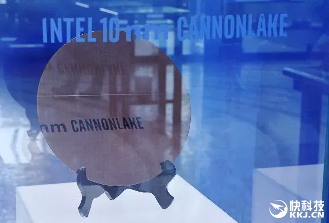
From http://news.mydrivers.com/
This is from the presentational display. Detail is very hard to make out at the highest resolution we can find this image.
Additional: 1:20pm September 19th
Intel has also now put the presentation up on the website, which gives us this close-up:

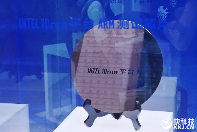
Surprisingly, this wafer looks completely bare. Either this is simply a 300mm wafer before production, or Intel have covered the wafer on purpose with a reflective material to stop prying eyes. It's a very odd series of events, as Intel did have other wafers at the event, including 10nm using ARM, and examples of the new 22FFL process.
From http://news.mydrivers.com/
 From http://news.mydrivers.com/
Both of these wafers seem to have a repeating pattern we would typically see on a manufactured wafer. So either Intel does not want anyone to look at 10nm Cannon Lake just yet, or they were just holding up an unused disc of silicon.
Additional: 3:00pm September 20th
Intel got back to us with a more detailed Cannon Lake image, clearly showing the separate dies:
Manual counting puts the wafer at around 36 dies across and 35 dies down, which leads to a die size of around 8.2 mm by 8.6 mm, or ~70.5 mm2 per die. At that size, it would suggest we are likely looking at a base dual-core die with graphics: Intel's first 14nm chips in a 2+2 configuration, Broadwell-U, were 82 mm2, so it is likely that we are seeing a 2+2 configuration as well. At that size, we're looking at around 850 dies per wafer.
Source: Intel


52 Comments
View All Comments
MajGenRelativity - Tuesday, September 19, 2017 - link
Joke? :PBrokenCrayons - Tuesday, September 19, 2017 - link
Joke and fact all at once! MrSpadge wins the Internet for today.MajGenRelativity - Tuesday, September 19, 2017 - link
Congratulations on your keys to the Internet! Please lock it away and then throw away the key :Pjjj - Tuesday, September 19, 2017 - link
They were claiming over 3.3GHz for A75 at 250uW per MHz so that's ok.Specs wise there was this slide http://img1.mydrivers.com/img/20170919/970972625ab...
peevee - Tuesday, September 19, 2017 - link
"using a new transistor counting methodology"What? +2 for each transistor? ;)
edzieba - Tuesday, September 19, 2017 - link
The new methodology = count total transistors per mm^2, rather than picking one arbitrary dimension of a certain axis of a certain process stage and judging everything by that.HStewart - Tuesday, September 19, 2017 - link
What it looks like, Intel is stacking the transistors on top of each, so size of die does not actual determining factor - but actually number of transistors is.edzieba - Tuesday, September 19, 2017 - link
No stacking involved. The dies are a single layer, and the 'extra' link dies are purely acting as interconnects.MrSpadge - Tuesday, September 19, 2017 - link
Designs use transistors of different sizes, depending on what they need to drive. The mobile SoC makers made Intel look bad with their densities, whereas the origin was that on average their applications required smaller transistors than Intels high-frequency designs. So Intel decided on some standardized transistor mix for these comparisons to give neither an advantage nor a disadvantage to anyone. Actual designs will differ in density, but that's true for any fab.name99 - Tuesday, September 19, 2017 - link
"some standardized transistor mix for these comparisons to give neither an advantage nor a disadvantage to anyone"Oh you naive little kitten. There's ALWAYS winners and losers from these sorts of decisions.
For example memory is more dense than logic. So a metric that privileges memory density over logic density makes a company that ships with lots of logic on the chip look worse. Even if your metric includes both memory and logic transistors, who's to say what the appropriate weighting is?
There are also higher level arguments. SoCs don't run by transistors alone. You need wiring to connect these; you need somewhat empty space between the transistors, you need clock distribution and pads connecting silicon to metal. Point is, all these things take space, and a metric that measures ONLY the size of a transistor does not capture how efficiently a process does or does nor use this extra space --- a more reasonable metric would cover a larger area.
What does Intel think about this?
"Simply taking the total transistor count of a chip and dividing by its area is not meaningful because of the large number of design decisions that can affect it–factors such as cache sizes and performance targets can cause great variations in this value"
Which I translate as "our individual transistors are tiny, so we're going to publicize that, but our tools for connecting them together suck, so we're not going to discuss how dense the transistors are where it actually MATTERS --- laid out on a real chip".
But don't worry, there are other metrics one can use!
FinFETs use multiple fins per transistor to attain high enough drive current. One of TSMC's goals is over the next few years to reduce the number of needed for most transistors for the current 3 or 4 down through 2 and ultimately to 1 (achieved in part by making each fin higher and higher and higher). So there's an easy out for Intel here --- switch to FIN density rather than TRANSISTOR density and, voila, Intel is immediately looking a whole lot better --- so many more fins per sq mm!