The Snapdragon 845 Performance Preview: Setting the Stage for Flagship Android 2018
by Ryan Smith & Andrei Frumusanu on February 12, 2018 12:30 AM EST- Posted in
- Mobile
- Snapdragon
- Qualcomm
- Smartphones
- SoCs
- Snapdragon 845
In what has become an annual tradition for Qualcomm, the company has once again opened the doors of their San Diego headquarters to the press to take a preview look at the next generation of their flagship mobile platform. These events have been going on for several years now, and have become an integral part of how Qualcomm approaches the public with their wares; preview events not only let them set expectations, but to get the word out to technically-minded audiences in a vendor-neutral manner. Rather than being one part in the next flagship smartphone, preview day means that everything can be about Qualcomm and the platforms that they have created.
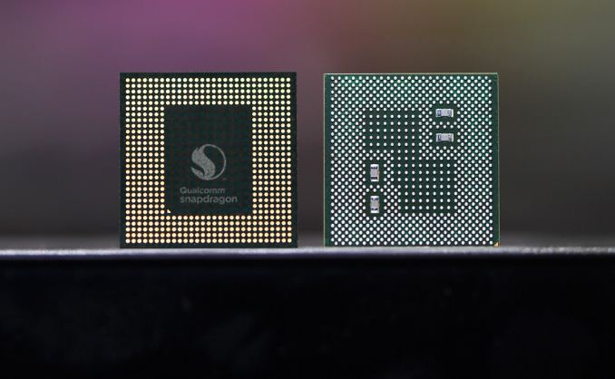
Late last year Qualcomm announced the Snapdragon 845 platform, the successor to 2017’s Snapdragon 835. Implementing a number of important architectural improvements over its predecessor, the Snapdragon 845 gets to follow-up on what ended up being a rather well-received platform in the Snapdragon 835, and to see if Qualcomm can maintain their momentum. Qualcomm used their December event to release a good bit of info on the 845 in advance, so we’ve already had a chance to see what Qualcomm is planning architecturally. And now with the preview event we finally get to see how all of this comes together with a look at the platform as a whole.
Whenever discussing the state of affairs of Qualcomm’s flagship SoCs, I always struggle not to tie it to the Snapdragon 810 in some fashion. Which not to beat Qualcomm over the head for past mistakes – in that case a poorly thought out response to Apple – but rather because it serves as a such a great point of reference for discussing the company’s SoC development as a whole. 810 was arguably the company’s low point, so everything since then has been part of a rather remarkable upward trajectory for the flagship Snapdragon. Even though Qualcomm has been leading the pack in high performance SoCs for several years now, last year’s Snapdragon 835 in particular really felt like Qualcomm was in that position for all-around technical capabilities and not merely because of size, momentum, and the realities of LTE licensing.
All of this means that there’s a lot riding on the Snapdragon 845, just in a different and less obvious way than before. Qualcomm has redeemed themselves from the 810 and it’s not a question of whether they can put together a great SoC, but instead it’s a question of how they will follow up upon a great SoC like the 835.
| Qualcomm Snapdragon 845 vs 835 | |||
| SoC | Snapdragon 845 | Snapdragon 835 | |
| CPU | 4x Kryo 385 Gold (A75 derivative) @ 2.8GHz 4x256KB L2 4x Kryo 385 Silver (A55 derivative) @ 1.77GHz 4x128KB L2 2MB L3 in DSU |
4x Kryo 280 Gold (A73 derivative) @ 2.45GHz 2MB L2 4x Kryo 280 Silver (A53 derivative) @ 1.90GHz 1MB L2 |
|
| GPU | Adreno 630 | Adreno 540 @ 670/710MHz | |
| Memory | 4x 16-bit CH @ 1866MHz LPDDR4x 29.9GB/s 3MB system cache |
4x 16-bit CH @ 1866MHz LPDDR4x 29.9GB/s |
|
| ISP/Camera | Dual 14-bit Spectra 280 ISP 1x 32MP or 2x 16MP |
Dual 14-bit Spectra 180 ISP 1x 32MP or 2x 16MP |
|
| Encode/ Decode |
2160p60 10-bit H.265 720p480 |
2160p30 (2160p60 decode), 1080p120 H.264 & H.265 |
|
| Integrated Modem | Snapdragon X20 LTE (Category 18/13) DL = 1200Mbps 5x20MHz CA, 256-QAM UL = 150Mbps 2x20MHz CA, 64-QAM |
Snapdragon X16 LTE (Category 16/13) DL = 1000Mbps 3x20MHz CA, 256-QAM UL = 150Mbps 2x20MHz CA, 64-QAM |
|
| Mfc. Process | 10nm LPP | 10nm LPE | |
The answer to that comes in the form of the Snapdragon 845, an interesting SoC that is a “tock” design if there ever was one. Qualcomm doesn’t get the advantage of an entirely new manufacturing node – the 845 is being made on Samsung’s second-generation 10LPP process, a refined version of 10LPE used for the 835 – so Qualcomm’s improvements are rooted almost entirely in architecture rather than a mix of architecture and manufacturing. Which is to say that it’s a bit of an uphill challenge for the company, but the flip side of that argument is that it’s going to be a chance for Qualcomm’s architectural engineers to take attention front and center.
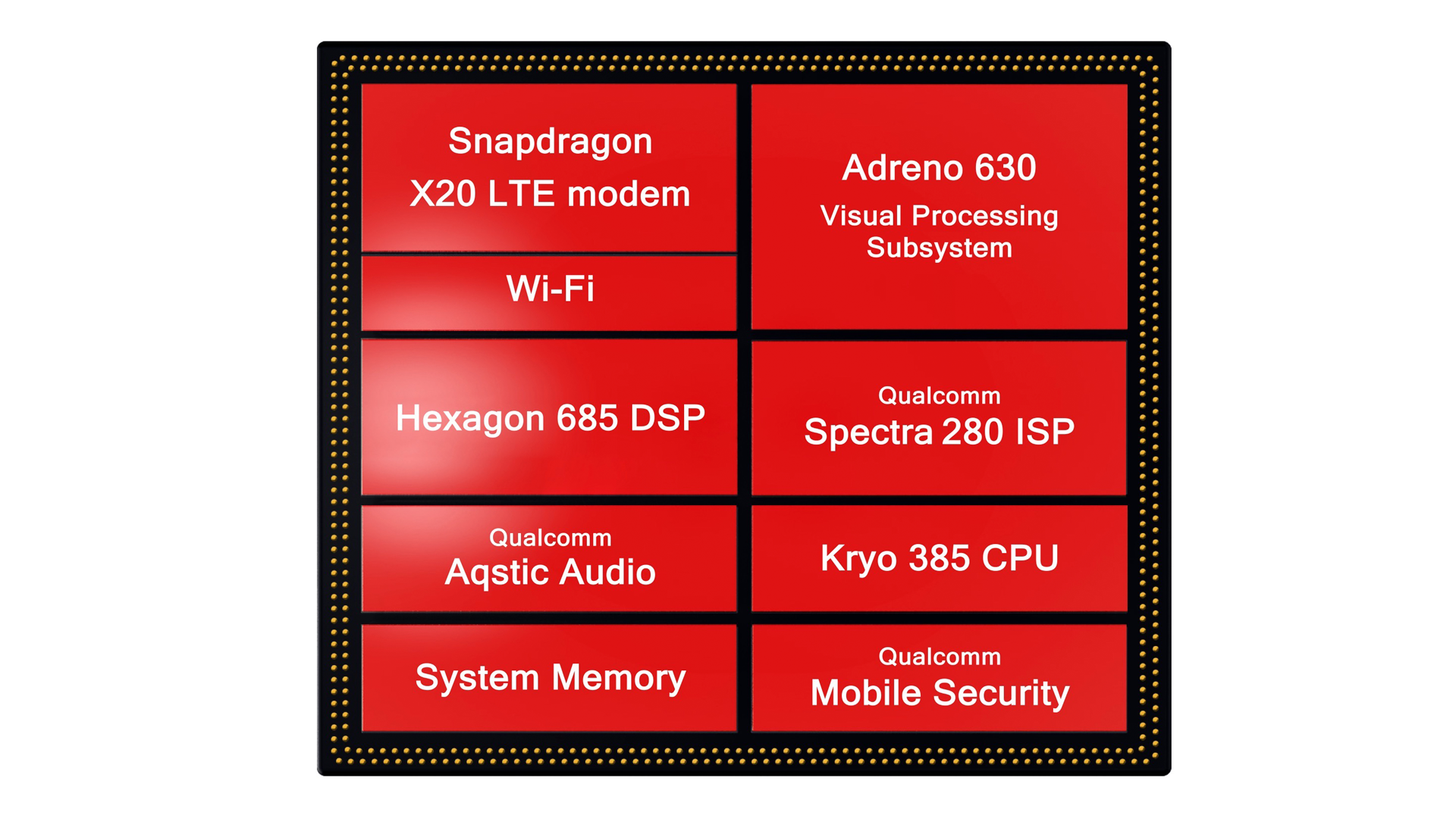
What the Snapdragon 845 entails then, as we originally learned late last year, is a series of upgrades and overhauls across all the various subsystems of the SoC. Arguably the biggest news here is that Qualcomm’s latest-generation Kyro 385-series CPU cores are derived from ARM’s Cortex-A75 and A55 designs, and that the resulting SoC is the first to employ ARM's DynamiQ CPU cluster organization. DynamIQ enables the various different CPU cores within an SoC to be hosted within the same cluster and cache hierarchy, as opposed to having separate discrete clusters with no shared cache between them, allowing for finer-grained and more efficient approaches to when and how various clusters are powered up. Meanwhile on the GPU side, the notoriously tight-lipped GPU group over at Qualcomm has confirmed that the Snapdragon 845 implements the first Adreno 600 series GPU, which in turn is the first new GPU architecture from Qualcomm in a couple of years and promises some significant performance improvements.
Outside of the core processor architecture, the changes in the rest of the SoC are perhaps not quite as dramatic, but still important to the platform as a whole. This includes, of course, Qualcomm’s latest and greatest LTE modem, the Snapdragon X20, upgrading Qualcomm’s LTE capabilities category 18. Both the camera ISP and Hexagon DSP have also been upgraded as well with the introduction of the Spectra 280 and Hexagon 685, which Qualcomm will be leveraging for camera image quality improvements and their stake in the modern mobile AI race respectively. Finally, the SoC also includes the latest version of the company’s Aqstic audio codec, which although audio has not traditionally been heavily promoted by the company, will be an increasingly important part of differentiating itself from other high-performance mobile SoCs.
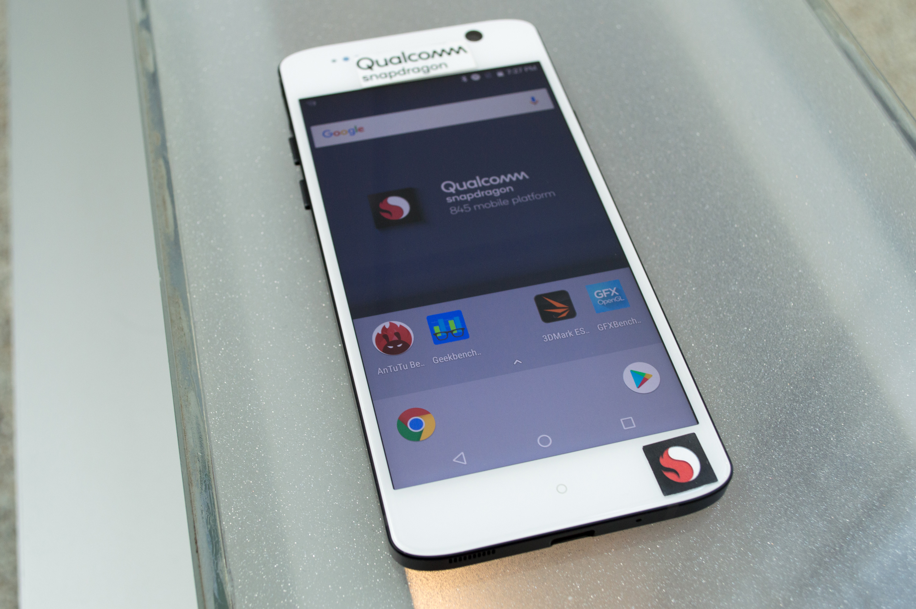
Getting down to the heart of matters then, this year’s flagship Snapdragon platform preview is a lot like last year’s. We’re once again taking a look at a Qualcomm Reference Design (QRD), which is a fully functional smartphones in a slightly oversized, utilitarian chassis used for hardware testing and software development. The Snapdragon 835 QRD was a 5.5-inch equivalent phone, and for the 845 QRD Qualcomm has stuck with much the same. The device itself is unremarkable, featuring a 1440p LCD and 6GB of LPDDR4X memory, but it’s otherwise typical of the class of Snapdragon 845 devices we expect to see starting a bit later this year.
Similarly, while this is still a preview, final device performance shouldn’t be too much different from what we see with Qualcomm’s QRD. Vendors do make customizations to both hardware and software, so how a device’s cooling system is built or how aggressive the power management is configured will have an impact on final performance. But as far as stock performance goes, the QRD is about as neural as it gets, if not a slightly idealized case for the platform as it allows Qualcomm to optimally configure the phone themselves.


140 Comments
View All Comments
BenSkywalker - Monday, February 12, 2018 - link
Legal studies I am lacking, you are correct, alas you can't keep out of the press how much trouble QC is in for their practices-https://www.forbes.com/sites/greatspeculations/201...
China fined them for a billion already, Korea for $850 Million, Taiwan for another $750 Million- US suit is in progress.
Andrei Frumusanu - Monday, February 12, 2018 - link
No I'm comparing the same methodology on the devices, active system power. The Shield TV on the X1 does 12W at 61fps. The QRD845 did 82fps at 4.4W.Nowhere in this article nor from Qualcomm is there the pure GPU power figure published, but always the system power. Your Nvidia figure is running at half performance meaning up to a 3x higher efficiency point. The GPU at full power is at 5-6W and that's why the Shield and Switch need an active fan to cool them.
The gap is not closed by process normalisation.
BenSkywalker - Monday, February 12, 2018 - link
Samsung says the gap is entirely closed by process normalisation alone(20nm<35%14nm<,40%10nmLPE<15%10nm LPE) , their claims- but hey, they just actually make the chips. What do the people who run the 10nm fab know compared to you, right?Three years later, they have a competitive part, you want to consider that a QC win, well, you are clearly their target customer. Spend more on lawyers, less on engineers :)
mfaisalkemal - Monday, February 12, 2018 - link
after calculate with samsung process normalisation, nvidia still have a gap around 20% worse than qualcomm on gfxbench 3.0 manhattan.Nvidia tegra x1 : 12W * 0.3315 = 3.978 W (Normalize from 20nm to 10nm)
61FPS @ 3.978W -->15.33FPS/W
Adreno 640
82FPS @ 4.4W --> 18.63FPS/W
mfaisalkemal - Monday, February 12, 2018 - link
i mean adreno 630 lolBenSkywalker - Monday, February 12, 2018 - link
Could you provide some links? Seems odd that the Adreno 640 uses the exact same wattage on two different benches.Also- your wattage consumption assumption negates the earlier link I provided showing a massive efficiency gain in terms of performance/watt once you moved away from nearing thermal limits. Either you would be able to clock the part higher at the same power level(reduced leakage, better matching of optimal power usage for the die etc) or you would use less power- not to mention you would no longer be using active cooling for something that low power(again reducing power draw).
That would assume, of course, that no other improvement was possible in the last *THREE YEARS* since we saw this level of performance.
BTW- We could also ask things like why is tessellation performance still *half* of a three year old SoC, but that would imply that Qualcomm actually cared about moving forward with technology.
mfaisalkemal - Monday, February 12, 2018 - link
that data was from Andrei Frumusanu comment, and i think he test it but not published. yup your're right nvidia better on tesselation offscreen test, but adreno 630 better on texturing offscreen(15424mtexel/s vs 13427mtexel/s) and i guess gfxbenchmark car chase test(tesselation test) adreno 630 better than tegra x1 although the tesselation offscreen worse.your link provided why so low wattage(1.51W) i think because nvidia only estimate gpu power without ram power, in this article andrei and ryan estimate system power(device substract idle power like display etc.
Kvaern1 - Tuesday, February 13, 2018 - link
I'd be much more disappointed with NVidia if Qualcomm could make GPUs as well as them.Now, if only NVidia could make a competitive CPU.
Eximorph - Tuesday, February 13, 2018 - link
I have the shield tv, shield k1 and an lg g5 ( tegra x1, tegra k1 and adreno 530) let me tell you that the tegra x1 is powerful but let's be honest. First The tegra x1 is connected to a power sources, second the tegra x1 is on max performance mode at all time, 3rd it have fans and 4th lets go to the specs, 256 cores at 1000 mhz vs 256 cores at 624 mhz on the adreno 530 we are talking about 376 mhz more per core for the tegra x1 over the adreno 530, screen resolution 1080 vs 2k. Now lets under clock the x1 to a 624 mhz and let put a 2k resolution screen and let see whats happen ? The result with just a 2k screen is the next one, Manhattan 3.0 offscreen, google pixel c 46 fps adreno 530 46 fps. So the true here is that Qualcomm is a beast on the gpu side and nvidia, apple and amr have alote to learn. Qualcomm is not behind, Qualcomm is far ahead. a really small chip with a really low power consumption and a great performance. The tegra x1 do not have nothing to look against the adreno 630.Eximorph - Tuesday, February 13, 2018 - link
https://wccftech.com/snapdragon-820-benchmarks/