The Snapdragon 845 Performance Preview: Setting the Stage for Flagship Android 2018
by Ryan Smith & Andrei Frumusanu on February 12, 2018 12:30 AM EST- Posted in
- Mobile
- Snapdragon
- Qualcomm
- Smartphones
- SoCs
- Snapdragon 845
CPU & Memory Subsystem
As we mentioned earlier, the Snapdragon 845 is the first SoC employing ARM’s new cluster technology DynamiQ. The different CPU cores are no longer hosted in dedicated cluster subsystems but are now integrated in a larger DynamiQ cluster. This change means that the cluster cache which to date was referred to as the L2 cache becomes the L3 cache and the individual CPU cores now receive a new private per-core L2. In the case of the Snapdragon 845, the Kryo 385 performance cores – derivative of ARM’s new A75 – are configured with 256KB L2 caches. The Kryo 845 efficiency cores, which are derivative of the A55, use 128KB L2 cache configurations.
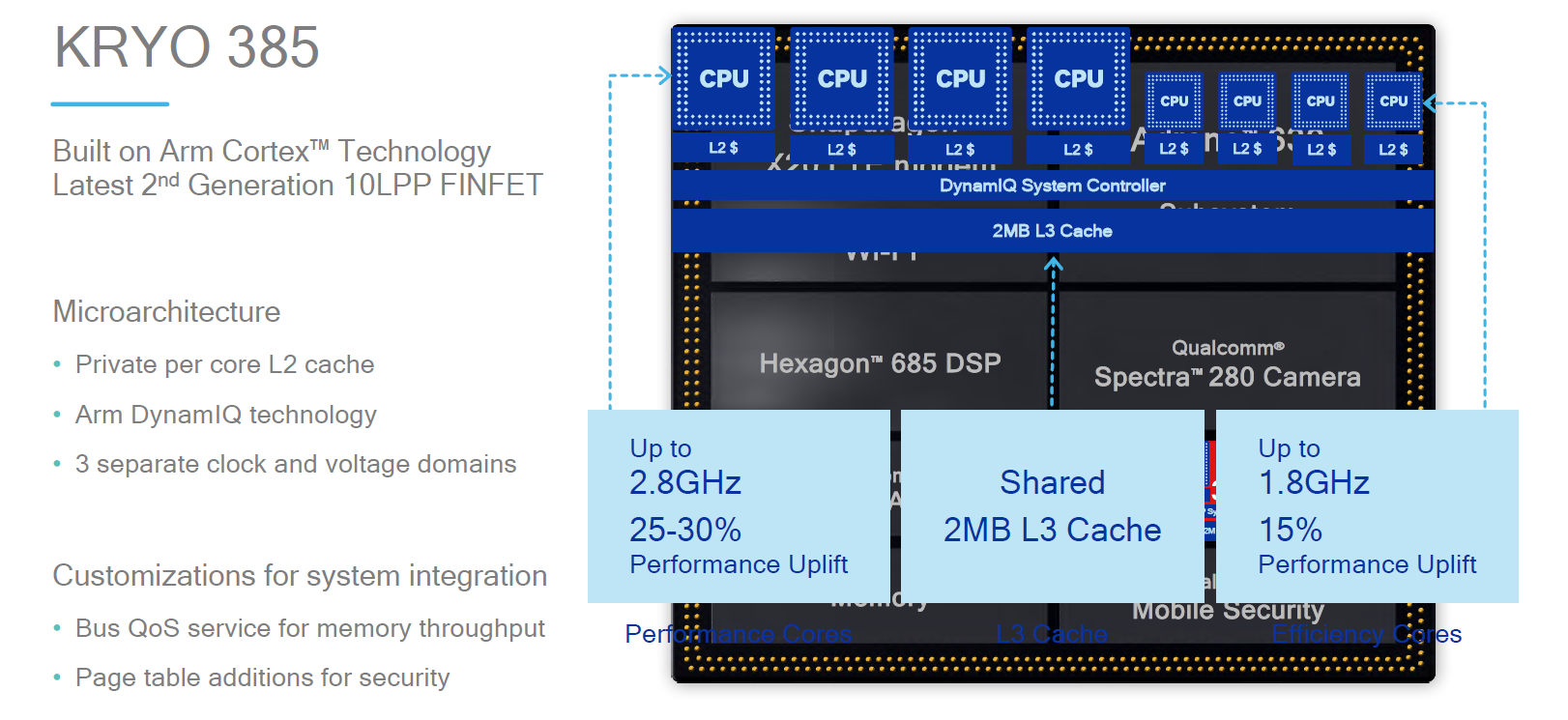
The L3 cache of the DynamiQ Shared Unit (DSU) is configured at 2MB. At the launch of the Snapdragon 845 Qualcomm advertised three voltage and clock domains – unfortunately we haven’t had time to look deeper into the system of the QRD to find out how this is partitioned, however it is still my unconfirmed belief that the third clock/voltage domain is dedicated to the DSU and not part of the CPU cores. An important characteristic that is totally new to the Android SoC ecosystem is the introduction of a system cache – this 3MB cache seems to sit at the memory controller / interconnect level above the CPU subsystem, something we’ll get back to in just a bit.
Qualcomm’s performance projections seemed relatively conservative as they claimed a performance uplift of only 25-30% which seemed lower than ARM’s projections. We have to keep in mind that beyond the microarchitectural improvements expected from the transition from A73 to A75 based CPU cores we also have a flat 14% frequency increase from 2.47GHz to 2.8GHz on the side of the performance cores. Unfortunately in the limited testing time we had with the QRD we couldn’t make use of long-running CPU benchmarks such as our SPEC suite, so for the scope of this article we had to base our synthetic analysis on GeekBench4 results.
| Geekbench 4 - Integer Performance Single Threaded |
|||
| Snapdragon 845 | Snapdragon 835 | % Increase |
|
| AES | 1160 MB/s | 942.5 MB/s | 23.1% |
| LZMA | 4.15 MB/s | 2.98 MB/s | 39.3% |
| JPEG | 20.8 Mpixels/s | 16.6 Mpixels/s | 25.2% |
| Canny | 32.1 Mpixels/s | 24.9 Mpixels/s | 28.8% |
| Lua | 2.18 MB/s | 1.75 MB/s | 24.0% |
| Dijkstra | 1.90 MTE/s | 1.62 MTE/s | 16.9% |
| SQLite | 70.3 Krows/s | 53.4 Krows/s | 31.8% |
| HTML5 Parse | 12.9 MB/s | 8.97 MB/s | 44.1% |
| HTML5 DOM | 3.00 Melems/s | 2.27 Melems/s | 31.9% |
| Histogram Equalization | 67.3 Mpixels/s | 52.5 Mpixels/s | 28.2% |
| PDF Rendering | 66.4 Mpixels/s | 48.5 Mpixels/s | 37.0% |
| LLVM | 321.2 functions/s | 257.3 functions/s | 24.8% |
| Camera | 7.96 images/s | 5.64 images/s | 40.9% |
For the integer workload results we see a healthy performance across the various tests. Qualcomm’s 25-30% increase here seems to be justified as this is the most common increase in most tests. Workloads such as LZMA, HTML5 parsing, PDF rendering and the Camera substests see larger increases into the 40% range. The overall improvement in absolute performance for the integer tests is 31%.
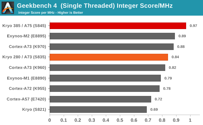
If we revisit performance per clock across recent microarchitectures we see the Snapdragon’s A75 based cores increase by only a meagre 15% which is below our expectations. We move on to the floating point benchmarks to see if we see a similar story.
| Geekbench 4 - Floating Point Performance Single Threaded |
|||
| Snapdragon 845 | Snapdragon 835 | % Increase | |
| SGEMM | 16.6 GFLOPS | 11.4 GFLOPS | 45.1% |
| SFFT | 4.23 GFLOPS | 2.86 GFLOPS | 47.9% |
| N-Body Physics | 1400 Kpairs/s | 872.2 Kpairs/s | 60.5% |
| Rigid Body Physics | 8524.2 FPS | 6130.5 FPS | 39.0% |
| Ray Tracing | 354.0 Kpixels/s | 232.7 Kpixels/s | 52.1% |
| HDR | 11.9 Mpixels/s | 8.31 Mpixels/s | 43.2% |
| Gaussian Blur | 34.5 Mpixels/s | 23.9 Mpixels/s | 44.3% |
| Speech Recognition | 17.9 Words/s | 13.6 Words/s | 31.6% |
| Face Detection | 752.4 Ksubs/s | 532.8 Ksubs/s | 41.2% |
The FP subtests of GB4 show a noticeably larger increase than the integer tests. Besides the switch from a 2-wide decode front-end to a 3-wide one, the largest changes of the A75 microarchitecture was found in the floating point execution pipelines and is likely the cause for the larger FP performance improvement. The boost here comes at an overall 45% in GB4.
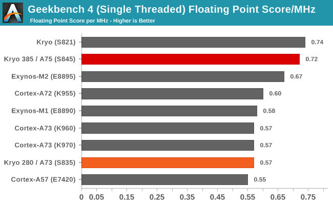
In terms of performance per clock, the 45% overall boost translates into a much larger 26% increase in IPC which is nearer to what we had expected.
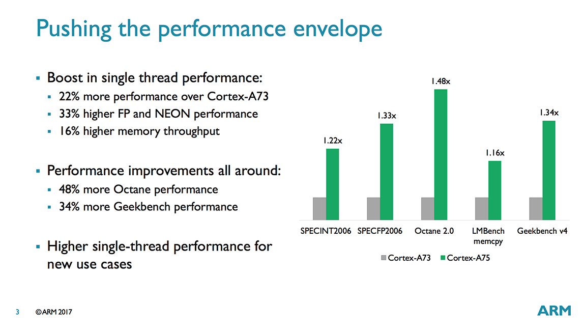
Revisiting the performance claims from ARM’s TechDay release of the A75 we notice that we had been promised larger improvements such as up to a 34% increase in GB4 performance per clock, which I interpreted with the frequency increase of the Snapdragon 845 to result in a 52% overall increase, which did not materialise. I reached out to ARM on the topic and got back several points of consideration: The projections ARM published were made on a A75 simulation with 512KB L2 caches and 2MB L3. The L3 matches the configuration of the Snapdragon 845 however Qualcomm’s choice of going with smaller L2 caches will have a certain performance hit. ARM didn’t have a number at hand for GB4 but quotes a 2% performance degradation for SPEC2000, and claims for GB4 it should be lower. Another consideration point is the memory subsystem of the SoC which ARM can’t control but heavily impacts the performance of the CPU, so let’s have a look at that.
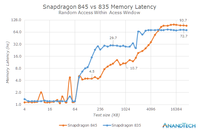
Running our internal memory benchmark on the QRD we see several expected characteristics of the Snapdragon 845: Compared to the Snapdragon 835’s A73 based cores we see the shift from shared cluster L2’s to private ones as well as the integration of sort of an L3 and L4 cache. The new L2 caches are very visible in our benchmark as memory latency up to the 256KB barrier (or rather, the 320KB barrier as the L1D and L2 are exclusive) sees a vast reduction compared to the L2 region of the A73 cores. The A75 cores promise 8-cycle hits for the L2 versus 19 cycles on the A73. In our test the difference is far larger as see a reduction from ~30ns down to ~4.5ns (not forgetting a clock frequency increase of the new cache). After the 256/320KB test size boundary we enter the DSU’s L3 cache. ARM describes the L3 as pseudo-exclusive so the outer boundary should end around or shortly after the 2048KB mark, the transition here is much harder to make out in the limited data we had time to collect so hopefully we’ll get to revisit it on a commercial device.
On the Snapdragon 835 the transition between L2 cache and DRAM is very sharp and visible in the graph. On the Snapdragon 845 however we see a far more gradient latency transition stretching out to up to the 5MB test depth. This is confirmation that Qualcomm’s system cache is indeed applied to the CPU subsystem and acts as an exclusive L4 cache to the processors. I think this new system cache is a true SoC-wide cache lying high up at the interconnect or memory controller level.
One of the worries of such a configuration for the CPU subsystem was increased latency to DRAM and it seems my fears were realised as the Snapdragon 845 shows a 30% increase in main memory latency from the CPU subsystem. Previously the Snapdragon 835 seemed to have by far one of the best memory controller implementations which directly resulted in higher performance of memory latency sensitive workloads. The latency increase in the 845 thus must be counteracting some of the microarchitectural improvements on part of the CPU cores. For GB4 in particular I made a remark that I didn’t notice any performance impact at all on the part of the Kirin 970’s memory latency, however we’re talking about different platforms and CPUs so I can’t be certain.
We reserve final conclusion on synthetic benchmarks until we get more time with a Snapdragon 845 device and able to investigate more and run SPEC. For now it looks like the Snapdragon 845 does not reach ARM’s projected performance levels, and falls well short of the claims. Among one of the other performance claims was Octane. We retired Octane some years ago and Google shortly followed up with official retirement, but as an added data-point the Snapdragon 845 reached a score of 15969 versus the Snapdragon 835’s 11879, also well short of a 20000 target that a projected 1.48x per clock performance increase would have resulted in.


140 Comments
View All Comments
BenSkywalker - Monday, February 12, 2018 - link
Legal studies I am lacking, you are correct, alas you can't keep out of the press how much trouble QC is in for their practices-https://www.forbes.com/sites/greatspeculations/201...
China fined them for a billion already, Korea for $850 Million, Taiwan for another $750 Million- US suit is in progress.
Andrei Frumusanu - Monday, February 12, 2018 - link
No I'm comparing the same methodology on the devices, active system power. The Shield TV on the X1 does 12W at 61fps. The QRD845 did 82fps at 4.4W.Nowhere in this article nor from Qualcomm is there the pure GPU power figure published, but always the system power. Your Nvidia figure is running at half performance meaning up to a 3x higher efficiency point. The GPU at full power is at 5-6W and that's why the Shield and Switch need an active fan to cool them.
The gap is not closed by process normalisation.
BenSkywalker - Monday, February 12, 2018 - link
Samsung says the gap is entirely closed by process normalisation alone(20nm<35%14nm<,40%10nmLPE<15%10nm LPE) , their claims- but hey, they just actually make the chips. What do the people who run the 10nm fab know compared to you, right?Three years later, they have a competitive part, you want to consider that a QC win, well, you are clearly their target customer. Spend more on lawyers, less on engineers :)
mfaisalkemal - Monday, February 12, 2018 - link
after calculate with samsung process normalisation, nvidia still have a gap around 20% worse than qualcomm on gfxbench 3.0 manhattan.Nvidia tegra x1 : 12W * 0.3315 = 3.978 W (Normalize from 20nm to 10nm)
61FPS @ 3.978W -->15.33FPS/W
Adreno 640
82FPS @ 4.4W --> 18.63FPS/W
mfaisalkemal - Monday, February 12, 2018 - link
i mean adreno 630 lolBenSkywalker - Monday, February 12, 2018 - link
Could you provide some links? Seems odd that the Adreno 640 uses the exact same wattage on two different benches.Also- your wattage consumption assumption negates the earlier link I provided showing a massive efficiency gain in terms of performance/watt once you moved away from nearing thermal limits. Either you would be able to clock the part higher at the same power level(reduced leakage, better matching of optimal power usage for the die etc) or you would use less power- not to mention you would no longer be using active cooling for something that low power(again reducing power draw).
That would assume, of course, that no other improvement was possible in the last *THREE YEARS* since we saw this level of performance.
BTW- We could also ask things like why is tessellation performance still *half* of a three year old SoC, but that would imply that Qualcomm actually cared about moving forward with technology.
mfaisalkemal - Monday, February 12, 2018 - link
that data was from Andrei Frumusanu comment, and i think he test it but not published. yup your're right nvidia better on tesselation offscreen test, but adreno 630 better on texturing offscreen(15424mtexel/s vs 13427mtexel/s) and i guess gfxbenchmark car chase test(tesselation test) adreno 630 better than tegra x1 although the tesselation offscreen worse.your link provided why so low wattage(1.51W) i think because nvidia only estimate gpu power without ram power, in this article andrei and ryan estimate system power(device substract idle power like display etc.
Kvaern1 - Tuesday, February 13, 2018 - link
I'd be much more disappointed with NVidia if Qualcomm could make GPUs as well as them.Now, if only NVidia could make a competitive CPU.
Eximorph - Tuesday, February 13, 2018 - link
I have the shield tv, shield k1 and an lg g5 ( tegra x1, tegra k1 and adreno 530) let me tell you that the tegra x1 is powerful but let's be honest. First The tegra x1 is connected to a power sources, second the tegra x1 is on max performance mode at all time, 3rd it have fans and 4th lets go to the specs, 256 cores at 1000 mhz vs 256 cores at 624 mhz on the adreno 530 we are talking about 376 mhz more per core for the tegra x1 over the adreno 530, screen resolution 1080 vs 2k. Now lets under clock the x1 to a 624 mhz and let put a 2k resolution screen and let see whats happen ? The result with just a 2k screen is the next one, Manhattan 3.0 offscreen, google pixel c 46 fps adreno 530 46 fps. So the true here is that Qualcomm is a beast on the gpu side and nvidia, apple and amr have alote to learn. Qualcomm is not behind, Qualcomm is far ahead. a really small chip with a really low power consumption and a great performance. The tegra x1 do not have nothing to look against the adreno 630.Eximorph - Tuesday, February 13, 2018 - link
https://wccftech.com/snapdragon-820-benchmarks/