The Samsung Galaxy S9 and S9+ Review: Exynos and Snapdragon at 960fps
by Andrei Frumusanu on March 26, 2018 10:00 AM ESTThe Snapdragon 845 - A Quick Recap
Starting with Qualcomm's Snapdragon 845 – we already extensively covered during the December launch announcement as well as Qualcomm’s traditional performance preview most recently in February.
| Qualcomm Snapdragon 845 vs 835 | |||
| SoC | Snapdragon 845 | Snapdragon 835 | |
| CPU | 4x Kryo 385 Gold (A75 derivative) @ 2.8GHz 4x256KB L2 4x Kryo 385 Silver (A55 derivative) @ 1.77GHz 4x128KB L2 2MB L3 @ 1478MHz |
4x Kryo 280 Gold (A73 derivative) @ 2.45GHz 2MB L2 4x Kryo 280 Silver (A53 derivative) @ 1.90GHz 1MB L2 |
|
| GPU | Adreno 630 @ 710MHz | Adreno 540 @ 670/710MHz | |
| Memory | 4x 16-bit CH @ 1866MHz LPDDR4x 29.9GB/s 3MB system cache |
4x 16-bit CH @ 1866MHz LPDDR4x 29.9GB/s |
|
| ISP/Camera | Dual 14-bit Spectra 280 ISP 1x 32MP or 2x 16MP |
Dual 14-bit Spectra 180 ISP 1x 32MP or 2x 16MP |
|
| Encode/ Decode |
2160p60 10-bit H.265 720p480 |
2160p30 (2160p60 decode), 1080p120 H.264 & H.265 |
|
| Integrated Modem | Snapdragon X20 LTE (Category 18/13) DL = 1200Mbps 5x20MHz CA, 256-QAM UL = 150Mbps 2x20MHz CA, 64-QAM |
Snapdragon X16 LTE (Category 16/13) DL = 1000Mbps 3x20MHz CA, 256-QAM UL = 150Mbps 2x20MHz CA, 64-QAM |
|
| Mfc. Process | 10nm LPP | 10nm LPE | |
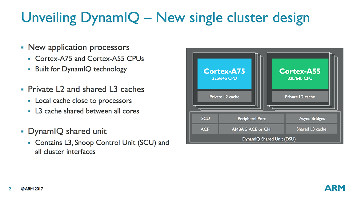
The Snapdragon 845 is the first SoC to adopt ARM’s new DynamIQ CPU topology and cores. The new configuration includes a larger coherent cluster instead of separate clusters for the little and big cores. While this new configuration allows for better performance and core configuration scaling, Qualcomm opted to continue the traditional 4+4 CPU set that we’ve seen with the Snapdragon 835. The performance core comprise of the Kryo 385 Gold cores which are derivative of ARM’s Cortex-A75’s and are running at up to 2803MHz. The efficiency cores are the Kryo 385 Silver cores which are based on ARM Cortex-A55’s and are running at up to 1766MHz.
Among the big improvements of the Snapdragon 845 includes the introduction of the new X20 modem which supports LTE UE Category up to 18 in the downstream and Category 13 in the upstream.
The Snapdragon 845 is also the first SoC from Qualcomm to adopt the new in-house designed Adreno 630 which marks a generational leap in the graphics department. I can confirm that Qualcomm continues the trend of trying to maintain clock frequencies between generations and the Adreno 630 in the Galaxy S9 comes in at 710MHz – a bump from the 670MHz in the Galaxy S8 but the same as other Snapdragon 835 devices. We’ll be having a more in-depth evaluation of the new Adreno in the GPU part of the review later on.
Unique for Android SoCs is also the first time introduction of a new system wide “L4” cache 3MB in size which is meant to reduce system memory access not only from the CPUs but also every other IP block in the SoC, thus gaining power efficiency.
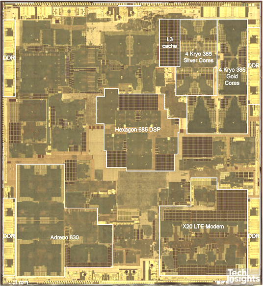
Snapdragon 845 Floor Plan. Image Credit TechInsights
Our friends at TechInsights this week were able to publish a die shot of the Snapdragon 845, and it’s interesting to see the changes compared to the Snapdragon 835. Because the Snapdragon 845 is manufactured on Samsung’s 10LPP process, there aren’t any new density improvements over last year’s 10LPE Snapdragon 835. Naturally because the new SoC includes new IP and improvements, die size has increased from 72.3mm² to around 94mm².
The biggest contributor of this increase will be the new system cache, which is part of the area that TechInsights (erroneously in my belief) marked as the DSP. Here we four new blocks to what I think are simply four banks of SRAM and their arbitration logic and their responsibility is divided among the four memory controller channels.
On the CPU side we see the new DSU lying in-between the A55 cores with the A75 cores spread around the little cores and the DSU. The 2MB L3 cache a big unified block alongside the DSU and little cores. Based on TechInsights preliminary low-res picture, the CPU complex comes in at 11.39mm² with an A75+L2 core coming in at 1.57mm² and the A55+L2 coming in at ~0.53mm².
The Adreno 630 seems to have consolidated a lot of its inner components. We still see a clear 4-shader core arrangement, however instead of having one adjacent block next each shader core we now see a larger block shared among two shader cores. The shader cores are also vastly improved as they have doubled the ALU pipelines. On the die shot it looks like the GPU actually only has 2 separate units, and this is confirmed by the drivers of the Snapdragon 845: instead of a quad-core Adreno 540, the Adreno 630 is a dual-core GPU. The texture units/ROPs/GMEM blocks have also been consolidated from four units down to two larger blocks, with a 50% increase in texture throughput. Overall there’s been extensive rework throughout the GPU resulting in a “simplified” configuration that seems to be forward-looking in terms of future scalability. Qualcomm has also achieved this in a mere ~10.69mm², making the Adreno 630 the by far smallest high-end GPU in the mobile space by a significant margin.
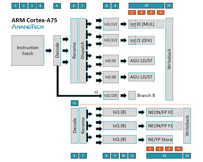
In terms of CPU performance, the new Kryo 385 Gold cores shouldn’t veer off much from ARM’s Cortex A75 microarchitecture. We’ve extensively covered the improvements in last year’s Tech Day reveal article. Overall the Cortex A75 is a strong successor to the A73 but refines the microarchitecture in terms of memory performance and especially floating point performance.
Following the performance preview of the Snapdragon 845 in February I noted that I was a bit disappointed in the end-performance of the CPUs as they did not reach ARM’s quoted performance targets. I want to revisit this a bit attempt to try to explain the different factors that lead to it.
Firstly ARM’s performance figures were projected on a configuration of A75 coupled with 512KB L2 caches. Qualcomm opted to use 256KB caches which may account for a few percentages in performance.
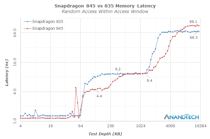
The new memory subsystem of the Snapdragon 845 also isn’t without faults: the initial increased DRAM memory latency that we measured on Qualcomm’s QRD845 reference platform is definitely carrying over to retail consumer devices, as the Galaxy S9 exhibits the same behaviour. This is quite a disappointing characteristic to find as it will counteract a lot of performance gains – especially in memory latency sensitive workloads – which we’ll confirm later on in the SPEC benchmarking portion.
Finally, one big question that Qualcomm teased about in its announcement event, is the configuration of the DSU. Qualcomm explained that the CPU complex was powered by three voltage planes – and I can confirm that my initial assessment was correct as two frequency and voltage planes power the little and big cores, and the third voltage plane powers the DSU/L3 and the cDSP (On of the various DSPs). The frequency here tops out at 1478MHz which is a tad lower than I had expected.
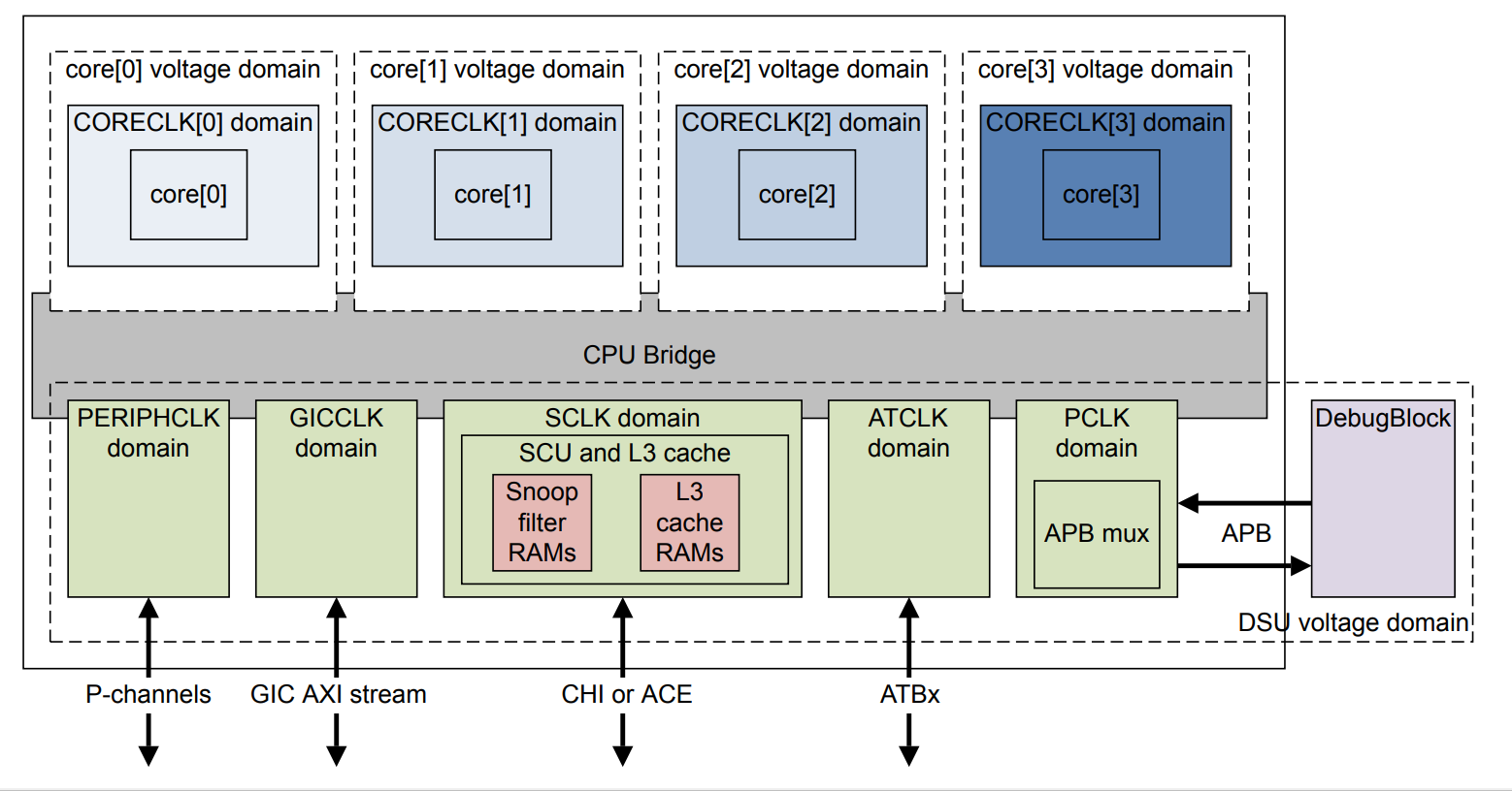
When reading ARM’s TRM (Technican Reference Manual) of the DSU, we see one particular claim regarding the recommended clocks of the L3 in relation to the CPU clocks:
"SCLK frequency affects the L3 hit latency and, therefore, it is important for achieving good performance. For best performance, ARM recommends running SCLK as close to CORECLK[CN:0] frequency as possible. However to reduce dynamic and leakage power, targeting a lower frequency might be required. Running SCLK at least approximately 75% of the CORECLK[CN:0] frequency might give an appropriate balance for many systems."
The Snapdragon’s big cores run at up to 2803MHz so running the L3 at up to only 1478MHz represents only 52% of the peak frequency. We’re not able to judge what kind of performance impact Qualcomm’s configuration has, but it looks like there will be some sort of degradation compared to an optimally run system.
All in all – the reduced 256KB cache, DRAM memory latency degradation as well as the more conservative maximum frequency of the L3 all can add up and may explain why the Snapdragon 845 wasn’t able to quite reach ARM’s projections on performance of the new core.
In general the Snapdragon 845 looks like a great SoC on paper – there should be good CPU improvements as well as excellent GPU leaps, but that’s no news given that we knew that from the performance preview. The only remaining question is power efficiency, which we’ll be looking at shortly after we cover the competition’s SoC.


190 Comments
View All Comments
generalako - Monday, March 26, 2018 - link
Android has had color management since Oreo, so get your facts straight. As for being able to device color modes, that's a different thing entirely, and is not and was not Samsung's way of dealing with color management, as you claim. That's just a made-up lie from your side. Allowing people to choose different color modes is actually a beneficial thing to have. With iOS, the target is to have color accurate images. So whatever images you see, they strictly follow sRGB or P3 gamuts. But on TouchWiz, Pixel UI, etc., people actually have the opportunity to choose more saturated colors, if that is to their liking. So they in essence provide an alternative in an area where Apple doesn't.Also, it needs to be stated that the S9 has the most color accurate display of any phone out there, as DisplayMate so very clearly noted and tested.
id4andrei - Monday, March 26, 2018 - link
I'm not saying that in its respective color profile the display is not good. I am talking about the OS. You the user are not supposed to choose color profiles. On ios you could have two images side by side, each targeting a different color profile, and the OS will display them correctly. In Android, you must manually switch profiles to match a photo while the other photo will look way off.generalako - Monday, March 26, 2018 - link
Except it isn't. The difference lies in the display drivers. Even Anandtech mention it in this article, about the black clipping, that Samsung ought to be able to be as good as well. Why? Because it's the same panel technology. So clearly the clipping isn't a result of hardware limitation, as is the case with LG's OLED panel in the V30 and Pixel 2 XL.DanNeely - Monday, March 26, 2018 - link
The big cores are about 3x the size of the small ones - "an A75+L2 core coming in at 1.57mm² and the A55+L2 coming in at ~0.53mm²" - I think you might be getting confused because the big core cluster wraps around the small ones in a backwards L shape, with 2 cores at the same height as the small ones and the second pair below.tipoo - Monday, March 26, 2018 - link
Rodger, was just going off what TechInsights had highlighted.tipoo - Monday, March 26, 2018 - link
Doh, I see now. The bottom line I was looking at is a SoC feature, not a white highlight box, I missed the end of the L.Commodus - Monday, March 26, 2018 - link
It's still fascinating to me that Qualcomm and Samsung alike seem to be losing ground to Apple -- aside from some of the graphics tests, the A11 fares better overall in cross-platform benchmarks. Used to be that there was some degree of leapfrogging between QC/Samsung and Apple, but the S845 and E9810 are really just catching up.goatfajitas - Monday, March 26, 2018 - link
Ogling over benchmarks and putting much weight into them is sooooooo 2006 ;)Quantumz0d - Wednesday, March 28, 2018 - link
True, Most of the talented developers at XDA nowadays focus more on the UX, Although there were a few long time back who had both but since Android changed a lot and the SoCs have increased in complexity, SD80x platform had bins and voltage control was easy but with the SD820 platform the voltage planes have increased even though can still be customized but need significant skill to micro optimize unlike the OMAP and the 800 and others.Apple is just banking on faux peak figures and OS knit with their tight integration optimizing for limited space of UI on iOS, they certainly have benefits but the downsides massively outweigh these advantages about the walled garden.
peevee - Friday, April 6, 2018 - link
"Apple is just banking on faux peak figures"They are not faux. If anything, the long-term testing in cooled environment is "faux", because nobody uses their smartphones as compute farms. When you start an app or open a webpage, the process runs for seconds at most, so that is what matters most in the CPU/memory/flash department. Only sustained performance which matters is games, on the GPU side of things.