The Samsung Galaxy S9 and S9+ Review: Exynos and Snapdragon at 960fps
by Andrei Frumusanu on March 26, 2018 10:00 AM ESTThe Snapdragon 845 - A Quick Recap
Starting with Qualcomm's Snapdragon 845 – we already extensively covered during the December launch announcement as well as Qualcomm’s traditional performance preview most recently in February.
| Qualcomm Snapdragon 845 vs 835 | |||
| SoC | Snapdragon 845 | Snapdragon 835 | |
| CPU | 4x Kryo 385 Gold (A75 derivative) @ 2.8GHz 4x256KB L2 4x Kryo 385 Silver (A55 derivative) @ 1.77GHz 4x128KB L2 2MB L3 @ 1478MHz |
4x Kryo 280 Gold (A73 derivative) @ 2.45GHz 2MB L2 4x Kryo 280 Silver (A53 derivative) @ 1.90GHz 1MB L2 |
|
| GPU | Adreno 630 @ 710MHz | Adreno 540 @ 670/710MHz | |
| Memory | 4x 16-bit CH @ 1866MHz LPDDR4x 29.9GB/s 3MB system cache |
4x 16-bit CH @ 1866MHz LPDDR4x 29.9GB/s |
|
| ISP/Camera | Dual 14-bit Spectra 280 ISP 1x 32MP or 2x 16MP |
Dual 14-bit Spectra 180 ISP 1x 32MP or 2x 16MP |
|
| Encode/ Decode |
2160p60 10-bit H.265 720p480 |
2160p30 (2160p60 decode), 1080p120 H.264 & H.265 |
|
| Integrated Modem | Snapdragon X20 LTE (Category 18/13) DL = 1200Mbps 5x20MHz CA, 256-QAM UL = 150Mbps 2x20MHz CA, 64-QAM |
Snapdragon X16 LTE (Category 16/13) DL = 1000Mbps 3x20MHz CA, 256-QAM UL = 150Mbps 2x20MHz CA, 64-QAM |
|
| Mfc. Process | 10nm LPP | 10nm LPE | |
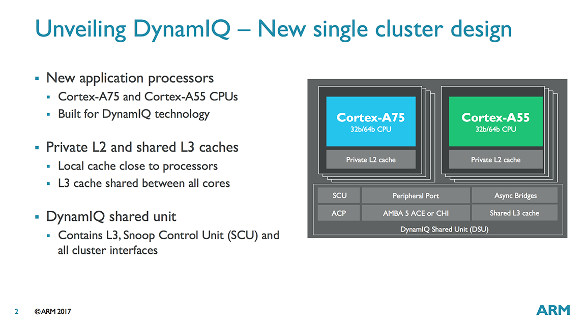
The Snapdragon 845 is the first SoC to adopt ARM’s new DynamIQ CPU topology and cores. The new configuration includes a larger coherent cluster instead of separate clusters for the little and big cores. While this new configuration allows for better performance and core configuration scaling, Qualcomm opted to continue the traditional 4+4 CPU set that we’ve seen with the Snapdragon 835. The performance core comprise of the Kryo 385 Gold cores which are derivative of ARM’s Cortex-A75’s and are running at up to 2803MHz. The efficiency cores are the Kryo 385 Silver cores which are based on ARM Cortex-A55’s and are running at up to 1766MHz.
Among the big improvements of the Snapdragon 845 includes the introduction of the new X20 modem which supports LTE UE Category up to 18 in the downstream and Category 13 in the upstream.
The Snapdragon 845 is also the first SoC from Qualcomm to adopt the new in-house designed Adreno 630 which marks a generational leap in the graphics department. I can confirm that Qualcomm continues the trend of trying to maintain clock frequencies between generations and the Adreno 630 in the Galaxy S9 comes in at 710MHz – a bump from the 670MHz in the Galaxy S8 but the same as other Snapdragon 835 devices. We’ll be having a more in-depth evaluation of the new Adreno in the GPU part of the review later on.
Unique for Android SoCs is also the first time introduction of a new system wide “L4” cache 3MB in size which is meant to reduce system memory access not only from the CPUs but also every other IP block in the SoC, thus gaining power efficiency.
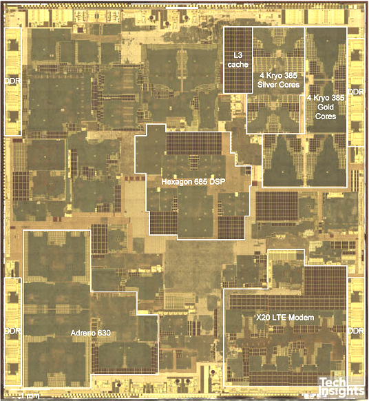
Snapdragon 845 Floor Plan. Image Credit TechInsights
Our friends at TechInsights this week were able to publish a die shot of the Snapdragon 845, and it’s interesting to see the changes compared to the Snapdragon 835. Because the Snapdragon 845 is manufactured on Samsung’s 10LPP process, there aren’t any new density improvements over last year’s 10LPE Snapdragon 835. Naturally because the new SoC includes new IP and improvements, die size has increased from 72.3mm² to around 94mm².
The biggest contributor of this increase will be the new system cache, which is part of the area that TechInsights (erroneously in my belief) marked as the DSP. Here we four new blocks to what I think are simply four banks of SRAM and their arbitration logic and their responsibility is divided among the four memory controller channels.
On the CPU side we see the new DSU lying in-between the A55 cores with the A75 cores spread around the little cores and the DSU. The 2MB L3 cache a big unified block alongside the DSU and little cores. Based on TechInsights preliminary low-res picture, the CPU complex comes in at 11.39mm² with an A75+L2 core coming in at 1.57mm² and the A55+L2 coming in at ~0.53mm².
The Adreno 630 seems to have consolidated a lot of its inner components. We still see a clear 4-shader core arrangement, however instead of having one adjacent block next each shader core we now see a larger block shared among two shader cores. The shader cores are also vastly improved as they have doubled the ALU pipelines. On the die shot it looks like the GPU actually only has 2 separate units, and this is confirmed by the drivers of the Snapdragon 845: instead of a quad-core Adreno 540, the Adreno 630 is a dual-core GPU. The texture units/ROPs/GMEM blocks have also been consolidated from four units down to two larger blocks, with a 50% increase in texture throughput. Overall there’s been extensive rework throughout the GPU resulting in a “simplified” configuration that seems to be forward-looking in terms of future scalability. Qualcomm has also achieved this in a mere ~10.69mm², making the Adreno 630 the by far smallest high-end GPU in the mobile space by a significant margin.
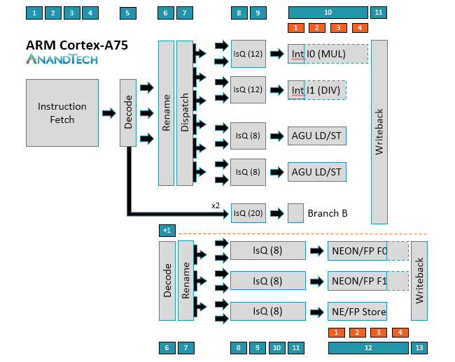
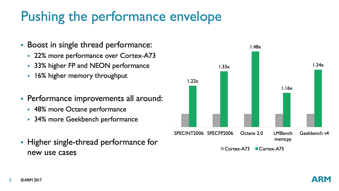
In terms of CPU performance, the new Kryo 385 Gold cores shouldn’t veer off much from ARM’s Cortex A75 microarchitecture. We’ve extensively covered the improvements in last year’s Tech Day reveal article. Overall the Cortex A75 is a strong successor to the A73 but refines the microarchitecture in terms of memory performance and especially floating point performance.
Following the performance preview of the Snapdragon 845 in February I noted that I was a bit disappointed in the end-performance of the CPUs as they did not reach ARM’s quoted performance targets. I want to revisit this a bit attempt to try to explain the different factors that lead to it.
Firstly ARM’s performance figures were projected on a configuration of A75 coupled with 512KB L2 caches. Qualcomm opted to use 256KB caches which may account for a few percentages in performance.
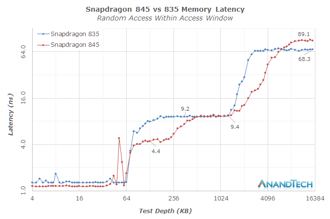
The new memory subsystem of the Snapdragon 845 also isn’t without faults: the initial increased DRAM memory latency that we measured on Qualcomm’s QRD845 reference platform is definitely carrying over to retail consumer devices, as the Galaxy S9 exhibits the same behaviour. This is quite a disappointing characteristic to find as it will counteract a lot of performance gains – especially in memory latency sensitive workloads – which we’ll confirm later on in the SPEC benchmarking portion.
Finally, one big question that Qualcomm teased about in its announcement event, is the configuration of the DSU. Qualcomm explained that the CPU complex was powered by three voltage planes – and I can confirm that my initial assessment was correct as two frequency and voltage planes power the little and big cores, and the third voltage plane powers the DSU/L3 and the cDSP (On of the various DSPs). The frequency here tops out at 1478MHz which is a tad lower than I had expected.
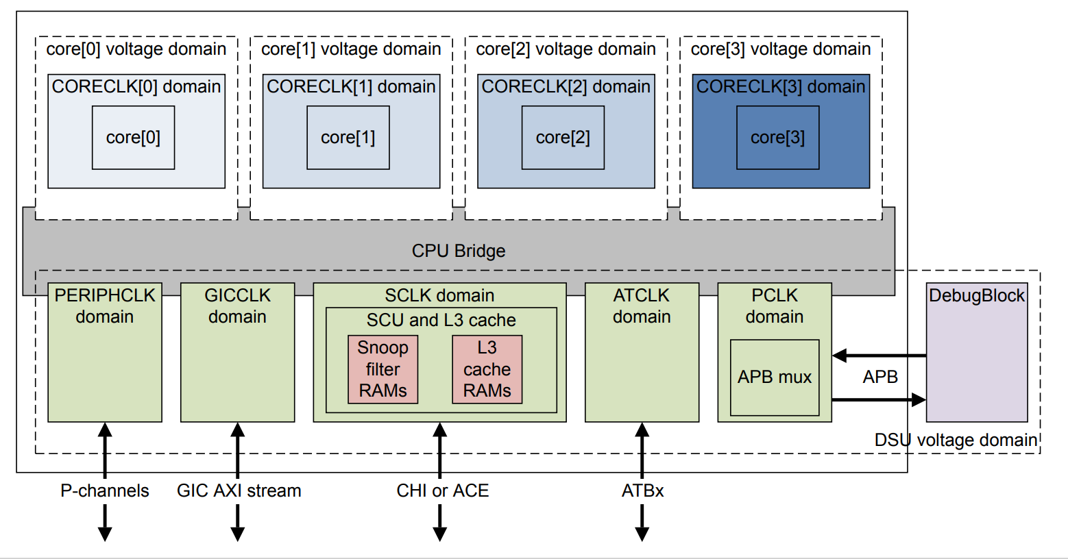
When reading ARM’s TRM (Technican Reference Manual) of the DSU, we see one particular claim regarding the recommended clocks of the L3 in relation to the CPU clocks:
"SCLK frequency affects the L3 hit latency and, therefore, it is important for achieving good performance. For best performance, ARM recommends running SCLK as close to CORECLK[CN:0] frequency as possible. However to reduce dynamic and leakage power, targeting a lower frequency might be required. Running SCLK at least approximately 75% of the CORECLK[CN:0] frequency might give an appropriate balance for many systems."
The Snapdragon’s big cores run at up to 2803MHz so running the L3 at up to only 1478MHz represents only 52% of the peak frequency. We’re not able to judge what kind of performance impact Qualcomm’s configuration has, but it looks like there will be some sort of degradation compared to an optimally run system.
All in all – the reduced 256KB cache, DRAM memory latency degradation as well as the more conservative maximum frequency of the L3 all can add up and may explain why the Snapdragon 845 wasn’t able to quite reach ARM’s projections on performance of the new core.
In general the Snapdragon 845 looks like a great SoC on paper – there should be good CPU improvements as well as excellent GPU leaps, but that’s no news given that we knew that from the performance preview. The only remaining question is power efficiency, which we’ll be looking at shortly after we cover the competition’s SoC.


190 Comments
View All Comments
Andrei Frumusanu - Monday, March 26, 2018 - link
I literally uploaded a 4K60 video on the S845 S9+. They always had it.https://youtu.be/9g88TIi-p2U
N Zaljov - Monday, March 26, 2018 - link
This article, as always, is some top-quality stuff. Really enjoyed reading it, Andrei!As for the CPU: Ah! Hotplugging! We finally meet again after all these years! How's it going ever since you've been banned from this planet? ;-)
Honestsly: I don't think that a company like S.LSI would seriously start fiddling around with deprecated mechanics like hot-plugging and slow asf DVFS scheduler settings, if there wouldn't be a major architectural/implementational flaw within the M3 cores.
This might sound like a far-flung theory, but could it be possible that there might be something wrong with the way how the M3 cores handle power-gating in a way that it just takes the CPU way too long to "warm up" cold blocks (like Register files, INT- & FP-Units etc.) that aren't utilized, which kind of translates into these terrible response times? While this might only explain the poor DVFS implementation, I don’t really find a reason why „hot-plugging“ should be the way to go for any sane semiconductor engineer or BSP developer.
Yes: It’s easier to implement and it costs less transistors (and wiring as well), but with modern process nodes, the added transistor budget simply wouldn’t even matter when you compare it with the huge amount of logic that’s there. In fact, I wouldn’t be too surprised if the hardware actually supports a more fine-grained control (with stuff like WFI for instance...), but at some point the BSP developers simply said „well, this stuff has already been working for us in the 5410 and 5420, so let’s go!“. Duh.
On the GPU side of things though, it doesn't look as bad as I initially suspected: S.LSI greatly increased their effort into improving perf/w of their Bifrost implementation, a big differentiationpoint between HiSilicon's last two generations and the appalling heap of junk of a GPU implementation in form of E8995's G71MP20.
Andrei Frumusanu - Monday, March 26, 2018 - link
> if the hardware actually supports a more fine-grained control (with stuff like WFI for instance...)WFI, core power down and cluster power down all work perfectly as intended and are being used. If they wouldn't be then this thing would melt. They use the hot-plugging just to force the scheduler. There's also no way to know which parts are of the S.LSI BSP and which parts are from the mobile division. I'm very sure all of this is likely mobile division additions however it can't be confirmed as they both use the same copyright name (Samsung Electronics) in the source files.
N Zaljov - Monday, March 26, 2018 - link
Thanks for clarifying. My apologies, I skipped the part that mentions "...to force thread migrations between the cores...".Another question: What software build is your S9 running on? The last update (afaik Build RC5) supposedly fixed some performance related issues and I was wondering, if they changed the bias of their governor (or at least tried it).
Andrei Frumusanu - Monday, March 26, 2018 - link
The review was done on ARC5.Quantumz0d - Wednesday, March 28, 2018 - link
Thanks for this Andrei, Also this article is pure gold !!Loved every bit of it from the Architecture to the benches, explanation, the wording, fantastic work there sir.
That Googles ridiculous decision to block Accessibility & the most essential 3.5mm jack mention and honest true facts about it in simplistic way yet hitting the bullseye, and the flow of the article is just marvellous art. Keep it up !!
One more thing I would suggest is, you might consider teaming up with Supercurio from XDA who built the Voodoo sound for Wolfson chips for Audio Analysis would be a great addition !!
Thank you again ! Looking forward for more.
tuxRoller - Monday, March 26, 2018 - link
The kernel has recently (https://lwn.net/Articles/737157/) completed a, nearly complete, rewrite of the hot-plugging core. This has made it both much faster and more reliable. So, it's very far from deprecated (though I won't speak to the way Samsung is using it here).Quantumz0d - Wednesday, March 28, 2018 - link
Exactly what I thought. After the SD810 the Hotplugging is very bad and inefficient. I wasn't surprised when the initial fantastic analysis was done by Andrei, but its really bad about the Battery life regression. Also I don't get this hype around the A series chips after that massive battery fiasco, they tune them so badly and look at the iPhone internals they barely have metal plate contact for heat transfer. Yeah I agree on the GPU part too surprised to see this. But I think Samsung wanted to have similar performance between the devices and down tuned the CPU in one and GPU in another...pure speculation.Apple manages to cheat always and damn all these idiotic sites who only show GB and say here's the Exynos and all. I didn't like how Samsung advertised the new SoC chip likes of Apple going for peak and not sustained.
I think that SD85x might have full custom cores like the OG Kryo from 820, I wish that to happen. Feels great to see how Adreno crushes the A11.
zer0hour - Monday, March 26, 2018 - link
Superb article, certainly of quality that lives up to the Anandtech name. I've been waiting for details of the E9810 S9 for ages, and this article is really the only one that explores the reasons for its weird real world vs synthetic performance.Speedfriend - Monday, March 26, 2018 - link
After seeing the S9 initial performance impressions and being in the UK, I decided to go for a pixel 2 XL for myself and an S8 to replace my gfs iPhone 6S. Very happy with both decisions, the pixel 2 XL is so fast and the S8 was a crazy deal.It is a real pity that performance and battery life are so hampered in the s9810 versions as I have loved my last few Samsungs. But if Google makes another good pixel this year, I can't see myself going back.