Western Digital: 96-Layer 3D NAND Progressing Well, Shipping to Retail Customers
by Anton Shilov on May 29, 2018 8:00 AM EST
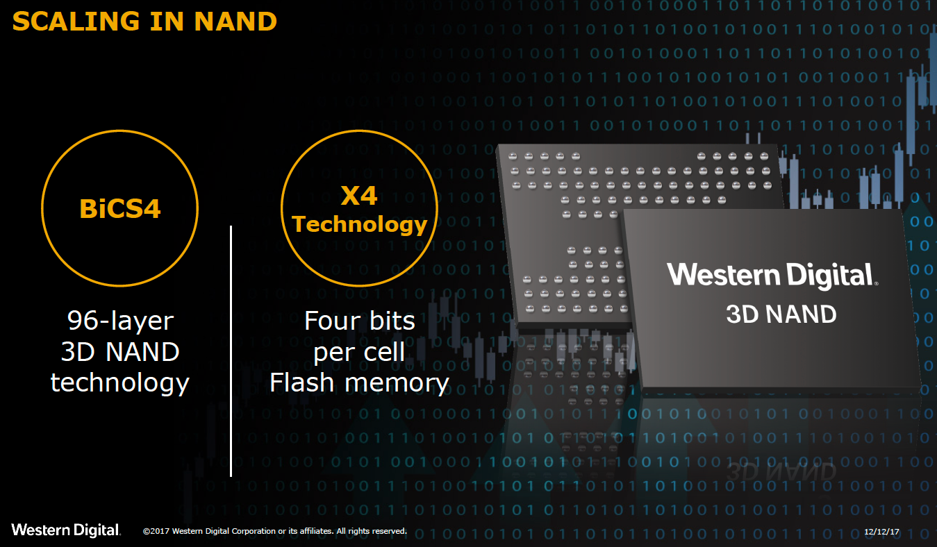
Western Digital this month said that it had started shipments of its fourth-generation BiCS 3D NAND memory to some of its customers. The company did not disclose details, but only said that the 96-layer 3D NAND memory is used for storage devices sold in retail, which usually means that it is used for inexpensive flash drives and/or memory cards. One of the important things about Western Digital’s BiCS4 memory is the manufacturer’s plan to build both TLC and QLC NAND using the technology.
Western Digital started production of its 96-layer BiCS4 NAND memory earlier this year and confirmed the beginning of the ramp up in late April during a conference call. At the J.P. Morgan Global Technology, Media and Communications conference in mid-May the company said that it had started to ship the said chips for revenue to its retail customers. Western Digital does not give any guidelines regarding the pace of the ramp up and the time when shipments of BICS4 exceed shipments of BICS3, but the fact that the ICs are used commercially is important.
“BiCS4, which is 96 layers, we have introduced that technology and we are shipping it primarily to our retail customers,” said Steve Milligan, CEO of Western Digital. “If you look to where we at from a yield curve perspective, because [BICS4] is not too mature, we are very pleased with where we are. Because once you get to a certain point, you can project where you are going to end at (based on cycles of learning, etc). So, the 96-layer technology is progressing quite well, we continue to increase output of that as we move to the rest of 2018, I am very thrilled and grateful for our strong 3D NAND execution.”
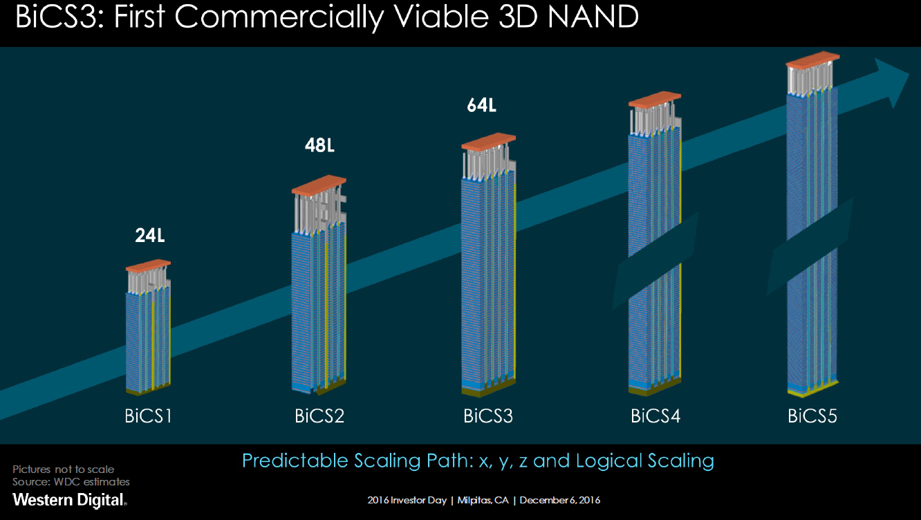
Western Digital’s (and Toshiba’s) BICS4 is a name for a family of 3D NAND flash devices featuring 96 active word lines (or layers). The lineup will include both TLC and QLC chips with capacities ranging from 256 Gb to 1 Tb. Based on Western Digital’s announcement from 2017, its first chips to use 96 word layers are 256 Gb 3D TLC NAND devices. After the manufacturer figures out how to produce 96-layer 3D NAND with sufficient yields, it will move on to higher-capacity 3D TLC and eventually 3D QLC chips with up to 1 Tb (128 GB) capacity.
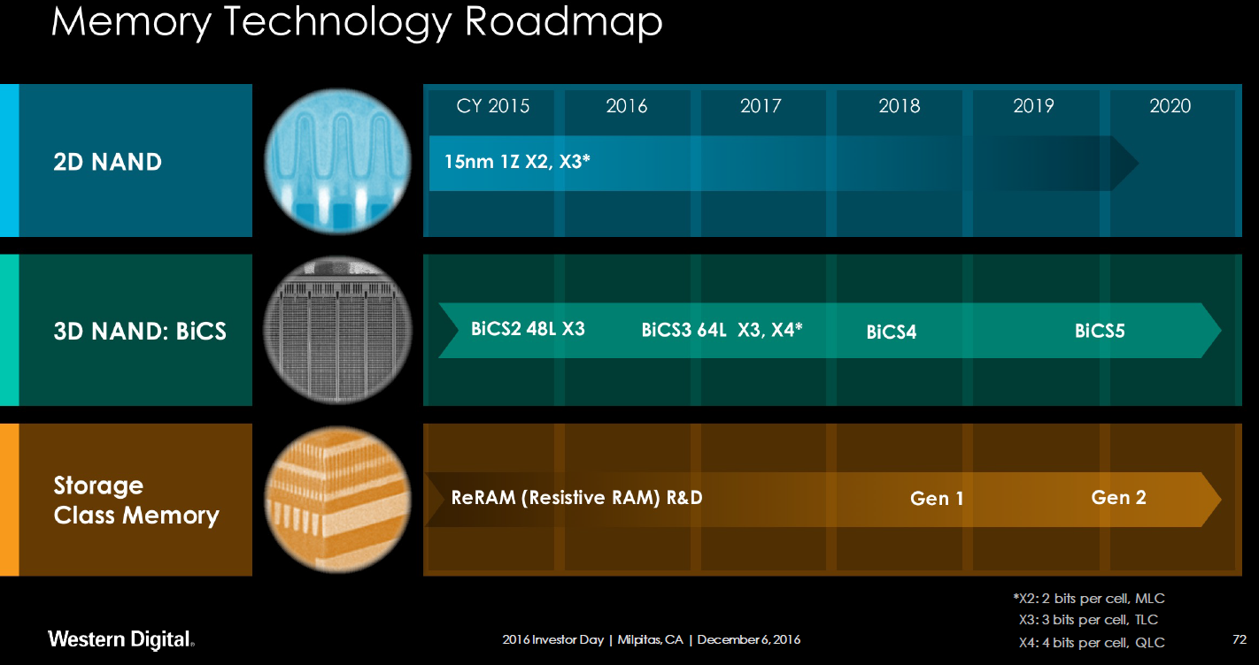
Speaking of QLC, it is necessary to point out that last year Western Digital and Toshiba also announced 768 Gb BICS3 64-layer 3D QLC NAND memory and it is highly likely that such ICs will hit the market earlier than 96-layer QLC NAND. Nonetheless, QLC is a crucial part of Western Digital’s future plans.
Related Reading:
- Western Digital Announce BiCS4 3D NAND: 96 Layers, TLC & QLC, Up to 1 Tb per Chip
- Western Digital Announces Four Bit Per Cell 64-Layer 3D NAND Flash
- Toshiba's 768Gb 3D QLC NAND Flash Memory: Matching TLC at 1000 P/E Cycles?
- Intel And Micron Launch First QLC NAND: Micron 5210 ION Enterprise SATA SSD
Source: Western Digital


29 Comments
View All Comments
dgingeri - Tuesday, May 29, 2018 - link
So, when are we getting the 3nm 2048 layer QLC 3D NAND?R0H1T - Tuesday, May 29, 2018 - link
So, when are we getting the 3nm 2048 layer QLC 3D NAND?2048 presumably!
Dragonstongue - Tuesday, May 29, 2018 - link
likely Samsung/TSMC will hit 3nm VERY soon, as far as "layers" are concerned, am sure the nm "shrinks" will hit a cannot pass plateau very soon (until beyond silicon is able to be done at a low cost such as pure optical to optical) so they may have to resort to "happy with 7nm or 5 or 3nm and instead add layer upon layer to increase durability/capacity and in a "round about" way endurance (data retention, P/E cycles)suppose in reality it was not that long ago we were at 150+nm, then 45nm, then 32-20-14-10 and very very soon 7nm, so it seems because of the massive $$$$$$$$$$$$$$ they are making on these things, the transitions to new tech is happening VERY rapidly indeed.
now 2048 layer.....HAHAHA, I do not picture this anytime soon, likely before they come to this point "layers" are likely to have been "ancient" technology done in the 2010s...I can picture in the ~2025 likely will be fairly close to being "optical" throughout (many companies have been working/refining this for the past decade or more)
peevee - Wednesday, May 30, 2018 - link
"likely Samsung/TSMC will hit 3nm VERY soon"They can "hit" it today, after all, these are just marketing names and have nothing to do with reality. But then they would need to invent and market a new naming scheme in a year or two, and their current "10nm" and "7nm" will be harder to sell.
jjj - Tuesday, May 29, 2018 - link
NAND went 3D because it hit the limit on horizontal scaling.2040 layers in 10-15 years if NAND survives for that long so no cheaper solution comes up.
There will likely be more than 4 bits per cell too by then.
eddieobscurant - Tuesday, May 29, 2018 - link
Is toshiba's/wd's 96-layer string stacking like intel's/micron's or a classic one like samsung's ?jjj - Tuesday, May 29, 2018 - link
lol see what happens if you aren't paying attentionThis was said on January 25 " Additionally, we commenced initial production of our 96-layer technology, BiCS4, and began product shipments to retailers in the December quarter. We expect to ramp BiCS4 in the second half of the calendar year. "
watzupken - Wednesday, May 30, 2018 - link
I think it is a meaningless race to produce a higher capacity SSD with significant deterioration of endurance. Understandably that even current TLC NAND, especially the 3D type in theory could last a very long time for most normal usage, but this leads to the next question, in terms of cost savings, I also question if QLC will be a significant savings over TLC SSDs.DanNeely - Wednesday, May 30, 2018 - link
They're hitting 1k P/E cycles with QLC, that's as good as a lot of first gen TLC flash; and outside of very write intensive work loads (which shouldn't be using cheap mass market SSDs anyway) will last long enough that something else failing will kill the drive before it hits its max wear level.