Samsung Foundry Updates: 8LPU Added, EUVL on Track for HVM in 2019
by Anton Shilov on September 6, 2018 11:00 AM EST
Samsung recently hosted its Samsung Foundry Forum 2018 in Japan, where it made several significant foundry announcements. Besides reiterating plans to start high-volume manufacturing (HVM) using extreme ultraviolet lithography (EUVL) tools in the coming quarters, along with reaffirming plans to use gate all around FETs (GAAFETs) with its 3 nm node, the company also added its brand-new 8LPU process technology to its roadmap.
10 nm Node Lives On
Samsung Foundry’s general roadmap was announced earlier this year, so at SFF in Japan the contract maker of semiconductors reiterated some of its plans, made certain corrections, and provided some additional details about its future plans.
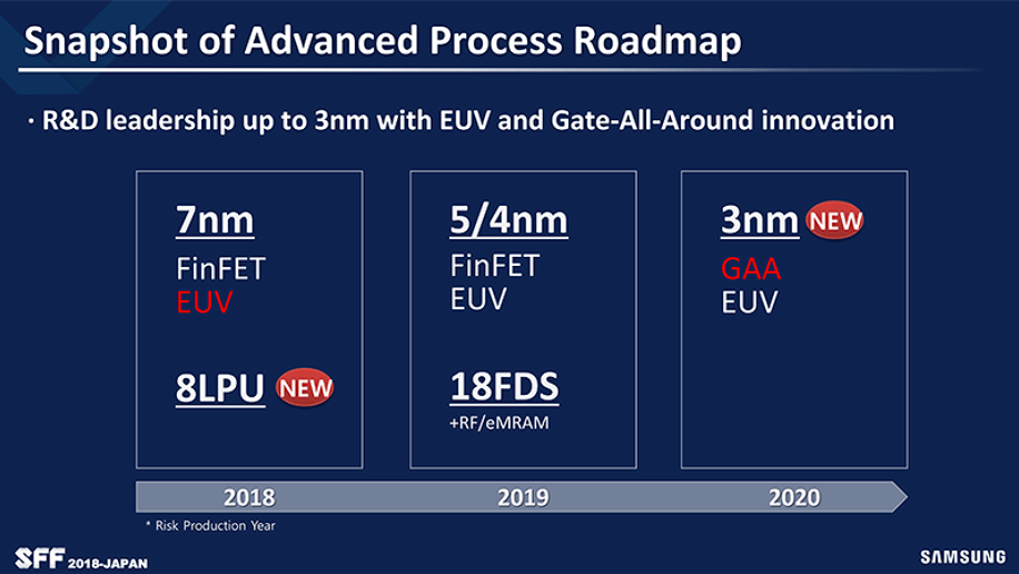
First up, Samsung added another fabrication technology into its family of manufacturing processes based on its 10 nm node. The new tech is called 8LPU (low power ultimate) and, according to Samsung’s usual classification, this is a process for SoCs that require both high clocks and high transistor density. Samsung’s 8LPP technology, which qualified for production last year, is a development of Samsung’s 10 nm node that uses narrower metal pitches to deliver a 10% area reduction (at the same complexity) as well as a 10% lower power consumption (at the same frequency and complexity) compared to 10LPP process. 8LPU is a further evolution of the technology platform that likely increases transistor density and frequency potential vs 8LPP. Meanwhile Samsung does not disclose how it managed to improve 8LPU vs. 8LPP and whether it involved advances of design rules, usage of a new library, or a shrink of metal pitches.
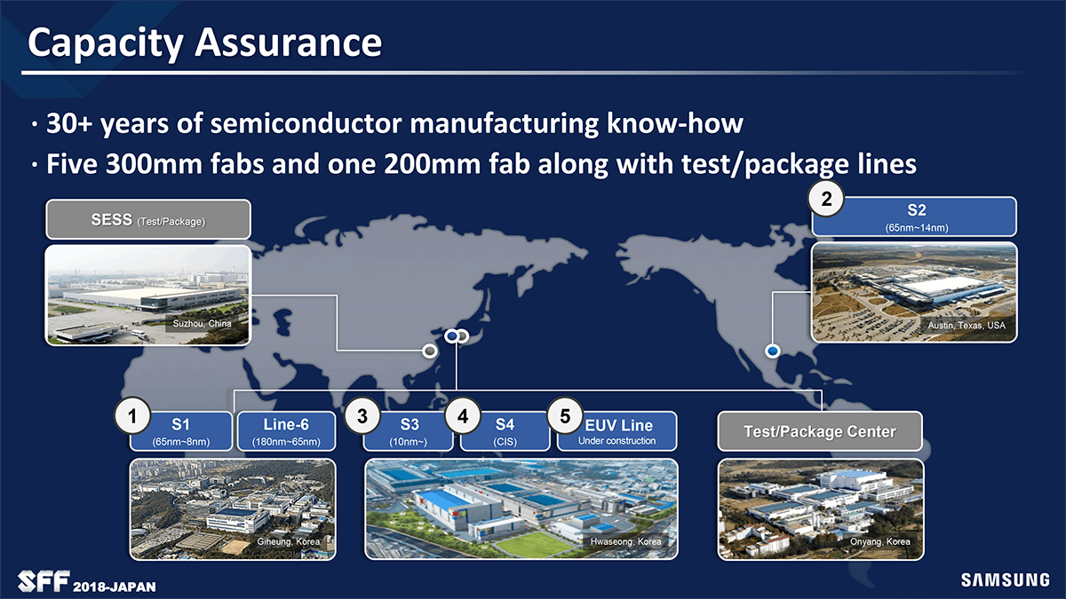
Samsung’s 8LPP and 8LPU technologies are aimed at customers who need higher performance or lower power and/or higher transistor density than what Samsung’s 10LPP, 10LPC, and 10LPU processes can offer, but who cannot gain access to Samsung’s 7LPP or more advanced manufacturing technologies that use EUVL. Risk production using 8LPU was set to start in 2018, so expect high-volume manufacturing to commence next year at Samsung’s Fab S1 in Giheung, South Korea.
7LPP EUV on Track
Last year Samsung Foundry promised to start risk production of chips using its 7LPP fabrication technology in 2018. As it appears, it has initiated manufacturing of certain 7LPP SoCs, though presumably only for its parent company, as its MPW shuttle service schedule does not mention 7LPP at all. The production tech will be Samsung Foundry’s flagship process, so expect the company to use it first for its parent company’s mobile SoCs. Meanwhile, the process tech is also suitable for larger chips aimed at HPC, ML, and AI markets (think CPUs, specialized SoCs, etc.). For example, Samsung is prepping specialized IP for appropriate chips, including 100 Gbps+ SerDes and other.
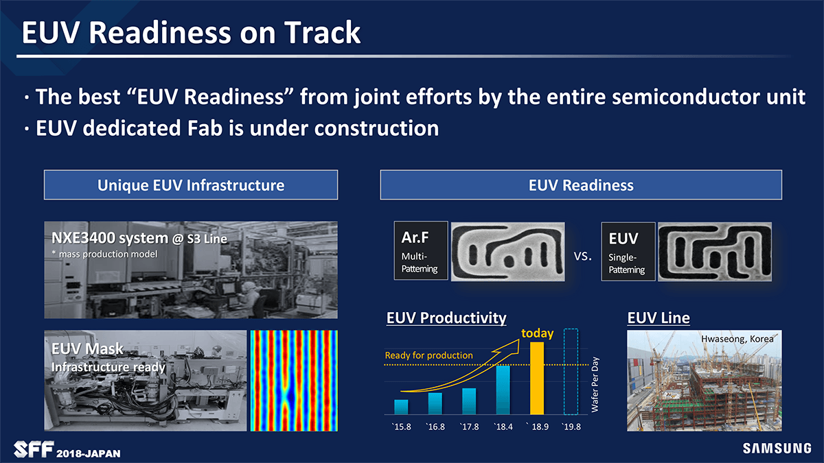
At the forum, Samsung Foundry said that it had installed multiple ASML Twinscan NXE:3400B EUVL step and scan systems at its Fab S3 in Hwaseong, South Korea. The company naturally does not disclose how many of such tools have been installed, but it indicated that wafer per day (WPD) performance of the said scanners is in line with its mass production targets. As reported before, the first manufacturing processes that will take advantage of EUVL will use it for select layers only, so do not expect extensive usage of the new equipment initially. In fact, since EUV will be used for HVM for the first time in the industry, Samsung Foundry is hardly inclined to expand its usage beyond select customers and designs (think Samsung Electronics and Qualcomm, which has already selected 7LPP for its Snapdragon 5G SoC due in 2019).
A radical expansion of EUV lithography usage by Samsung Foundry will occur after it builds another production line in Hwaseong, which will be architected for the EUV equipment from the start. The line is set to cost 6 trillion Korean Won ($4.615 billion), it is expected to be completed in 2019, and start HVM in 2020. As a result, Samsung’s production involving EUVL equipment will be limited to one fab for at least several quarters down the road. Generally, this is a reason why Samsung Foundry has developed its 8LPP and 8LPU process technologies.
5/4 nm to Hit Risk Production in 2019
By the time the new production line in Hwaseong becomes operational, Samsung Foundry promises to start risk production using its 5/4 nm node. As reported earlier this year, Samsung is prepping 5LPE, 4LPE, and 4LPP fabrication technologies, but eventually this list will likely expand. Based on what Samsung has disclosed about all three manufacturing processes so far, they will have certain similarities, which will simplify migration from 5LPE all the way to 4LPP, though the company does not elaborate.
One of the slides the company demonstrated at SFF 2018 Japan indicates that Samsung expects risk production of chips using the 5/4 nm node to commence in 2019, indicating that the process technologies will coexist rather than follow each other. Since there are hardly any reason for Samsung to design competing fabrication processes, it is more likely that its 5LPE will be used for HVM first in 2020 and then 4LPE/4LPP will follow later on expanding usage of EUV equipment, unless Samsung’s roadmap changes significantly and certain offerings get canned (which tends to happen).
One of the things to keep in mind is that Samsung’s 5/4 nm will be the company’s last node to use FinFET transistors, which is why it will be “long” node that will be used for many years to come, just like the 28 nm technology is used today and will stay here for a long time.
3 nm Pulled In?
One of the unexpected things that Samsung Foundry announced was start of risk production using its 3 nm node already in 2020, which is at least a year ahead of what was expected earlier. Samsung’s 3 nm will be the first node to use the company’s own GAAFET implementation called MBCFET (multi-bridge-channel FETs) and will officially include at least two process technologies: 3GAAE and 3GAAP (3nm gate-all-around early/plus).
Samsung still did not announce any HVM targets for 3GAAE and 3GAAP and it is hard to say when exactly the company adopts its MBCFET-based technologies for commercial SoCs. What we do understand today is that both technologies will rely on EUVL, so before using either Samsung will have to make sure that EUV delivers the necessary yields and production performance. Considering the fact that Samsung is satisfied with performance of its ASML Twinscan NXE:3400B EUVL step and scan systems today and expects further increases of WPD productivity, it is possible that it pulled in its 3 nm node.
18FDS Risk Production Due in 2019
Although GAAFETs are only several years away, technologies based on planar transistors are not going anywhere and keep evolving. Samsung Foundry will continue to back FD-SOI technology going forward and will offer a formidable rival for GlobalFoundries’ 22FDX and 12FDX offerings.
Samsung Foundry intends to start risk production of chips using its 18FDS already in 2019, so expect HVM in 2020 at the latest. The tech uses the same BEOL interconnects as Samsung’s 14LPE/14LPP technologies (i.e., BEOL originally developed for its 20 nm planar process), but with new transistors and FEOL. The company promises that when compared to its 28FDS, its 18FDS will enable a 20% higher performance (at the same complexity and power), a 40% lower power (at the same frequency and complexity), and a 30% lower die area.
What is particularly important is that 18FDS will support both RF and eMRAM, allowing Samsung Foundry to target a wide variety of applications that require RF and embedded memory in the 5G era in 2020 and onwards.
3D System-in-Package Ready in 2019
Chip packaging technologies are gaining importance these days as it becomes increasingly hard and expensive to integrate everything into a single processor. Samsung (just like TSMC and GlobalFoundries) already has a number of package solutions for complex products, such as FOPLP-PoP for mobile SoCs and I-Cube (2.5D) for chips that use HBM2 DRAMs. Next year the company will offer its 3D SiP (system-in-package) solution that will enable it to pack a variety of devices into a single three-dimensional package with a small footprint.
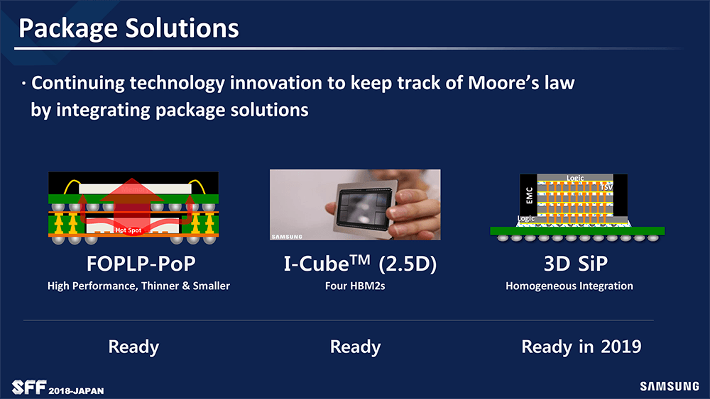
Samsung Foundry’s 3D SiP will be one of the industry’s first technology of its kind that will be used to build heterogeneous 3D SiPs (currently all SiPs are 2D). The package solution will enable the contract maker of semiconductors to assemble SiPs using components made using entirely different process technologies.
Related Reading:
- Samsung Foundry Roadmap: EUV-Based 7LPP for 2018, 3 nm Incoming
- Arm and Samsung Extend Artisan POP IP Collaboration to 7LPP and 5LPE Nodes
- Samsung’s 8LPP Process Technology Qualified, Ready for Production
- Samsung and TSMC Roadmaps: 8 and 6 nm Added, Looking at 22ULP and 12FFC
- TSMC Details 5 nm Process Tech: Aggressive Scaling, But Thin Power and Performance Gains
- Intel Delays Mass Production of 10 nm CPUs to 2019
- TSMC Kicks Off Volume Production of 7nm Chips
- TSMC Starts to Build Fab 18: 5 nm, Volume Production in Early 2020
Source: PC Watch


29 Comments
View All Comments
V900 - Thursday, September 6, 2018 - link
Whoops, forgot to post these links in my reply.https://pocketnow.com/7nm-technology-transition
https://appleinsider.com/articles/18/09/04/develop...
V900 - Thursday, September 6, 2018 - link
Nah... By the time Samsung get their process up and running, they won’t be able to for financial reasons:*Samsung will have invested billions into their 7nm node(s).
*The market for 7nm is pretty small compared to the overall market. It’s too expensive, only a limited amount of customers need (or can afford to pay for) that kind of performance.
*Samsung will want to recoup their investment. That’s less likely to happen if they license it out.
Death666Angel - Friday, September 7, 2018 - link
Depends on the licensing terms and that's up to the negotiating parties. If the therms are beneficial to both parties, why not? After licensing it in a few years, it will also take a while to order the necessary machines and ready a fab, so it's not like they will be immediate rivals. As I understand the GloFo situation, they are doing nothing 7nm related anymore, so it would make sense to license it, once Samsung has recouped most of the initial investment or is on a newer node already. Pretty sure every node advance in the last decade or more has cost billions to research, so that's no reason why they won't license it out.Morawka - Thursday, September 6, 2018 - link
Intel's lithography advantage appears to be on its deathbed. They wasted too much time on 10nm.iwod - Thursday, September 6, 2018 - link
TSMC Roadmap2018 - 7nm
2019 - 7nm+
2020 - 5nm ( Half EUV )
2021 - 3nm ( Full / Most EUV )
2022 - likely be a refined 3nm+
You can literally bet all these will be shipped to a big customer in Dozen millions of unit at September every year. So there are no Risk Production or HVM word play, they are the deadline which is done and shipped as final product.
porcupineLTD - Friday, September 7, 2018 - link
Yeah, because samsung invented those terms.Santoval - Friday, September 7, 2018 - link
I wonder how Samsung will manage the "trapped heat" of their 3D SiP, which is the greatest hurdle to their design and production. Whether HBM dies are used on top of logic or multiple logic dies on top of each other (as is shown in their graphic), how can the heat of the low and middle layers be removed?Is this solely intended for very low power mobile SoCs, clocked at <1.5 GHz but ending up being faster than single die normally clocked ones due to the much higher transistor count? Or are they going to employ elaborate cooling between the dies based on microfluidics?
boeush - Friday, September 7, 2018 - link
Microfluidics is one idea. An alternative might be to sandwich some heat-spreading layers in between those stacked dies - copper plates, or graphene, or something like that - to pipe the heat away into some overarching heatsink. But yeah, an interesting engineering challenge either way - and something I've been wondering about ever since Moore's Law began to sputter out in earnest.Anymoore - Sunday, September 30, 2018 - link
I just noticed on the capacity slide 7nm or under was not mentioned at all under any of the current fabs. 8nm was put under S1, which seems to be an older fab(?).