AMD Unveils ‘Chiplet’ Design Approach: 7nm Zen 2 Cores Meet 14 nm I/O Die
by Anton Shilov on November 6, 2018 1:53 PM EST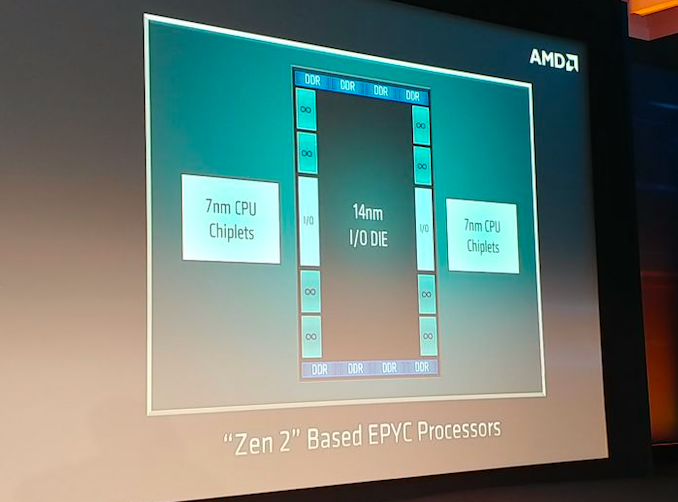
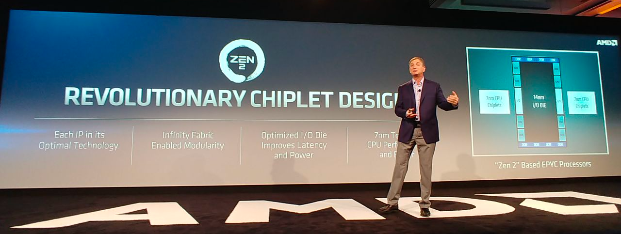
AMD on Tuesday disclosed some additional details about its upcoming codenamed Rome processor based on its Zen 2 microarchitecture. As it turns out, the company will use a new design approach with its next-generation EPYC CPUs that will involve CPU ‘chiplets’ made using TSMC’s 7 nm manufacturing technology as well as an I/O die made using a 14 nm fabrication process.
AMD’s chiplet design approach is an evolution of the company’s modular design it introduced with the original EPYC processors featuring its Zen microarchitecture. While the currently available processors use up to four Zen CPU modules, the upcoming EPYC chips will include multiple Zen 2 CPU modules (which AMD now calls ‘chiplets’) as well as an I/O die made using a mature 14 nm process technology. The I/O die will feature Infinity Fabrics to connect chiplets as well as eight DDR DRAM interfaces. Since the memory controller will now be located inside the I/O die, all CPU chiplets will have a more equal memory access latency than today’s CPU modules. Meanwhile, AMD does not list PCIe inside the I/O die, so each CPU chiplet will have its own PCIe lanes.
Separating CPU chiplets from the I/O die has its advantages because it enables AMD to make the CPU chiplets smaller as physical interfaces (such as DRAM and Infinity Fabric) do not scale that well with shrinks of process technology. Therefore, instead of making CPU chiplets bigger and more expensive to manufacture, AMD decided to incorporate DRAM and some other I/O into a separate chip. Besides lower costs, the added benefit that AMD is going to enjoy with its 7 nm chiplets is ability to easier bin new chips for needed clocks and power, which is something that is hard to estimate in case of servers.
This is a breaking news. We are updating the news story with more details.
Source: AMD


76 Comments
View All Comments
Hul8 - Tuesday, November 6, 2018 - link
AMD will be using the AM4 socket until 2020, so I doubt there will be more lanes for mainstream Ryzen. Never mind the market for such solutions is so tiny that AMD are better off offering Threadripper for those customers, instead of saddling even low-end with more cost.Spunjji - Friday, November 9, 2018 - link
This. Also they're moving up to PCIe 4.0 so the bandwidth available from fewer lanes on the desktop isn't really a concern.Targon - Wednesday, November 7, 2018 - link
Gen-Z, which AMD has been involved with since its inception, is what you are looking at. Look up Gen-Z consortium. I expect 2020 or 2021 when AMD will incorporate Gen-Z support into its processors/chipsets.marsdeat - Tuesday, November 6, 2018 - link
What does the "IO" area on the IO die actually mean? Each chiplet seems to have an IF link (8 chiplets at 8 cores each, there are 8 ∞ links on the IO die). I would not be surprised if the PCIe is what is being communicated by "IO", along with other controllers on-board.The controller die is huge by the looks of it, bigger than the full Zen 1 Zeppelin die by a large margin.
I'd be very interested to see how this comes to pass on Matisse, Renoir, and Castle Peak, but for Rome I still feel like the PCIe is on that controller die.
Hul8 - Tuesday, November 6, 2018 - link
I agree that the I/O on the I/O die is PCIe 4.As to why they didn't just call them "PCIe 4": The lanes can probably work in either PCIe 4 *or* 2nd Gen Infinity Fabric mode. After all, that's the way Socket-Socket communication was arranged on 1st Gen EPYC.
marsdeat - Tuesday, November 6, 2018 - link
RIGHT! I knew there was something I was forgetting, and it was how dual-socket EPYC support works. Thanks for reminding me!Yeah, IO makes sense when you think that's referring to dual-purpose ∞/PCIe bandwidth options. (Plus if there's an onboard SATA controller and all that jazz, that'll be in part of the IO section, I'm sure.)
Last-level cache could easily be on the IO die too, but I feel like calling it the "IO die" rather than "controller" or some other more vague term implies that it's also the PCIe node.
ravyne - Tuesday, November 6, 2018 - link
I'm thinking along the same lines as you two. the IO blocks probably are configurable as either the PCIe 4.0 or off-chip InfinityFabric.Thinking about it some more, I think its likely that there's some kind of large cache in the IO chip, but also L3 retained in the chiplet. They claim to get 2x density on 7nm, but they doubled core-count and doubled the SIMD compute width, register file, and data-path. Those 7nm chiplets somehow still look smaller than Zen1 dies. Its possible the DRAM controllers/pins can account for the difference, but it might be that L3 cache didn't stay at 2MB/core and that's what makes the chiplet < 2x area -- maybe its 8MB still, or 10, or 12, but not 16; it was fully-associative/victim cache in zen1, so it can be any size, really.
A lot of enterprise workloads, like databases, respond *really* well to huge caches, that's why IBM puts them in Power, and they also support/have-supported really large memory by having off-chip memory controllers with 64MB caches, and multiple of these controllers in a system. But your typical workstation workloads (CAD, Modelling, Rendering) don't respond so dramatically, much less consumer workloads. A 128MB cache in the IO die makes sense for the server market, and at the same time, an 8-core chiplet with 8MB L3 wouldn't need additional cache on the IO die in an APU (today's APUs already only have 1MB/core L3).
A potential worry here, is whether AMD will continue supporting things like ECC in IO dies bound for consumer SKUs (I hope so), or whether things like PCIe 4.0 will come to consumer SKUs as quickly as in enterprise SKUs (again, I hope so).
Overall though, this is a great strategy -- On the enterprise side, so much of board/system validation has to do with IO/Board interfaces. Moving compute onto chiplets means the computational cores can evolve on their own without invoking the full validation burden it normally would. In the future, we might only see one set of IO dies per socket for its entire lifetime, but new micro-architectures every 12-18 months, instead of alternating between process-shinks and new archs. Same goes for GPU chiplets on the consumer side -- no need to tie a particular CPU micro-architecture to a particular GPU micro-architecture, they can evolve at their own pace.
mczak - Tuesday, November 6, 2018 - link
I agree with others that i/o on the i/o die most likely refers to pcie.As for cache, good questions... I would assume L1/L2 are still to Zen - and as such I'd suspect there's value in having L3 shared by the cores on each chiplet, without having to go to the i/o die (cache also shrinks extremely well, so no need to really skimp on that there).
Although I wouldn't be surprised if there's an L4 cache in the i/o die - this thing appears rather huge, and while it's definitely very much non-square (increasing the circumference compared to area), apart from the interface logic and the actual PHYs (which need to be to toward the edges of the die) it's basic function is basically that of a router, and I think it could easily have enough area for rather large amounts of L4 (say, 128MB or so). But it remains to be seen...
abufrejoval - Wednesday, November 7, 2018 - link
From what I understand about the IF, PCIe is simply one of the protocols spoken on the IF fabric: You switch a bit it talks PCIe. But that doesn't mean you can drive PCIe level signals off the chiplets IF pins, that's where the amplifiers in the I/O hub comes in handy.If that I/O die actually acts as a configurable switch or if it is more of a hub, is one of the fun things I am looking forward to read about here.
FreckledTrout - Tuesday, November 6, 2018 - link
So does anyone think we will see a single CCX / chiplet design in the Ryzen lineup? Seems doable now the IO / memory is disconnected from the CCX / chiplet.