AMD Previews EPYC ‘Rome’ Processor: Up to 64 Zen 2 Cores
by Anton Shilov on November 6, 2018 2:27 PM EST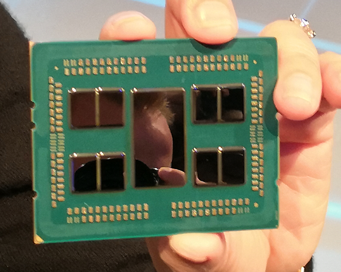
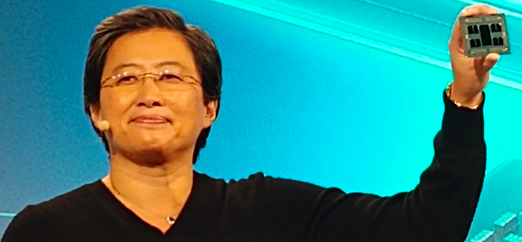
AMD on Tuesday formally announced its next-generation EPYC processor code-named Rome. The new server CPU will feature up to 64 cores featuring the Zen 2 microarchitecture, thus providing at least two times higher performance per socket than existing EPYC chips.
As discussed in a separate story covering AMD’s new ‘chiplet’ design approach, AMD EPYC ‘Rome’ processor will carry multiple CPU chiplets manufactured using TSMC’s 7 nm fabrication process as well as an I/O die produced at a 14 nm node. As it appears, high-performance ‘Rome’ processors will use eight CPU chiplets offering 64 x86 cores in total, as well as an eight-channel DDR4 memory controller supporting up to 4 TB of DRAM per socket. Besides, the new processor supports 128 PCIe 4.0 lanes to connect next-generation accelerators, such as the Radeon Instinct MI60 based on the Vega 7nm GPU.


Considering the fact that Zen 2 microarchitecture is expected to generally increase performance of CPU cores (especially when it comes to floating point performance, which AMD expects to double), the Rome processors will boost performance of servers quite dramatically when compared to existing machines. In particular, AMD expects performance per socket to double as a result of higher core count, and predicts that floating point performance per socket will quadruple because of arhitectural IPC improvements and increase of the core count.
One important peculiarity of AMD’s EPYC ‘Rome’ processor is that it is socket compatible with existing EPYC ‘Naples’ platform and will be forward compatible with AMD’s future ‘Milan’ platforms featuring CPUs powered by the Zen 3 microarchitecture. This will greatly simplify development of AMD-based servers and will enable server makers to reuse their existing designs for future machines, which is important for AMD that needs to capture market from Intel. To do that, it has to simplify job of server builders by making its platforms simple.
AMD is currently sampling its EPYC ‘Rome’ processor with server makers and customers. The company plans to launch ‘Rome’ products sometimes in 2019, but it does not disclose its launch schedule just now.


This is a breaking news. We are updating the news story with more details.


67 Comments
View All Comments
Xajel - Wednesday, November 7, 2018 - link
TR4 socket is just an SP3 socket physically. But electrically it's different.AMD used it because Threadripper was a last minute idea that Papermaster/Lisa liked and gave the green light for. They wasn't sure if it will be a success or not to put resources into a new platform nor they have time to make a one in the beginning.
So they just reused the SP3 socket, added few changes to the SP3 platform to make it consumer friendly & viola.
I expect it to last till the next major socket change (DDR5), then they will have a new platform & socket dedicated to the HEDT using a much smaller socket which should bring more benefits too like smaller size, lower cost & better compatibility with current/popular cooling solutions duo to it's smaller size.
liquidaim - Tuesday, November 6, 2018 - link
you make an intriguing observation. If we look at the fact that the MI60 card has infinity fabric allowing 200 GB/s transfers between GPUs, I can imagine these geniuses using that fabric to do exactly what you said for a 24 to 36 core gpu with good compression etc and high speed DDR4.It looks as though the I/O block is ~ 400mm2. Which seems freakishly large for just some I/O. If it also has some cache on it, it would be the perfect pairing with a gpu...
Hul8 - Tuesday, November 6, 2018 - link
Well it has to have 8 Infinity Fabric interfaces for the core chiplets, plus controllers for 8 memory channels, plus 128 PCIe lanes worth of PCIe4/IF2 connectivity, plus the SATA and USB ports.Compare 8/8/128 to 2/2/24 and you quickly see that it makes absolutely no sense to use the same I/O die for mainstream Ryzen as EPYC. If AMD even uses such a distributed design for regular Ryzen, its I/O die will be much smaller.
SaturnusDK - Wednesday, November 7, 2018 - link
The IO block is probably larger than it specifically needs to be in order to make a modular design where you can take the EPYC2 IO controller, cut it exactly in half and have 2 Threadripper 3rd gen IO controllers, or cut it in 4 and have 4 Ryzen 3rd gen IO controllers.nandnandnand - Tuesday, November 6, 2018 - link
At first Ryzen was 4-8 cores, Threadripper was 8-16 cores. Then Threadripper moved to 12-32 cores, which is a broad range. And that was Zen+, before Zen 2 and the new "chiplets".If 16-core Ryzen doesn't happen immediately, then I would be surprised if they didn't at least put out a 10 or 12-core Ryzen, maybe holding off 16 cores for a little later.
abufrejoval - Wednesday, November 7, 2018 - link
That's what I have been dreaming about since the first Zen launch!Santoval - Tuesday, November 6, 2018 - link
A 16-core Ryzen 2 will be highly memory starved due to the two channels of DRAM. AMD could do this but it would be unwise. On the other hand they *did* double the cores of Threadripper. 32 cores with quad channel memory is the same (in DRAM per core) as 16 cores with dual channel memory.It appears that they moved to an 8-core CCX for Epyc, so I wonder if they'll do they same for Ryzen 2 (with the option of having 8 cores with one CCX and 10 to 16 cores with two of them) or design an additional 6-core CCX for 12 cores max.
CodingRays - Wednesday, November 7, 2018 - link
Why would they have to create an additional 6core chiplet? Id expect them to use the chiplets with one or more defect cores. That way they could easily cover the entire 12-4 core range with one design. Also i hope that they are going to ditch the 4core cpu. That would put a bit more pressure on the industryoutsideloop - Tuesday, November 6, 2018 - link
And what is the 7nm Picasso APU gonna look like? Integrate the Vega (nay Navi) on the I/O chip, I would assume? But that would mean the GPU would be on 14/12nm? hmmmmSaturnusDK - Wednesday, November 7, 2018 - link
The recently revealed Vega mobile (or Radeon Pro Vega 16/20 to be exact) for the Mac Pro line up is on 14nm produced by TSMC so it would be logical to use that as the base for the APU part. Either separately or integrated in the IO controllers. Most likely the former.