The Ice Lake Benchmark Preview: Inside Intel's 10nm
by Dr. Ian Cutress on August 1, 2019 9:00 AM EST- Posted in
- CPUs
- Intel
- GPUs
- 10nm
- Core
- Ice Lake
- Cannon Lake
- Sunny Cove
- 10th Gen Core
Intel's new Ice Lake platform is the company's second attempt at producing a 10nm chip for the mass market, and follows on from the Cannon Lake platform. Using 'the same but different' 10nm process, Ice Lake holds inside a new 10th Gen Core microarchitecture called Sunny Cove, Gen11 graphics, and support for LPDDR4X-3733 as well as Thunderbolt and Wi-Fi 6. In advance of systems coming onto the market, Intel gave a small number of press a day of hands-on time with its Software Development Systems so we could get a taste of performance of Sunny Cove, Gen11, and Intel's newest 10nm product.
A Quick Recap on Ice Lake: Intel’s New Tick+Tock
For the best part of a decade, Intel was on it’s a strategy known as Tick Tock. For every new product family and generation, it would be known as a Tick or a Tock. For any Tick, the same core design was used on a new manufacturing process node, such as moving from 45nm to 32nm. For any Tock, the same process node was used as the previous generation, but we saw a new core design and microarchitecture, such as moving from Ivy Bridge to Haswell.
Intel stayed on this Tick Tock strategy from 2006 to around 2017, when it appeared that its 10nm process node technology was to be delayed. The company moved from a two-step cadence in Tick Tock to a 3-step cadence called Process Architecture Optimization. This is essentially Tick Tock, but with another step of Optimization on the end. Unfortunately, that plan quickly unravelled, as we ended up with multiple Optimizations based on the Skylake microarchitecture built on 14nm: Kaby Lake, Kaby Lake-R, Coffee Lake, and Coffee Lake-R, not to mention the mobile space which also received Amber Lake and Whiskey Lake. Technically Intel did release a Process update in H1 2018 with Cannon Lake on 10nm, but that was a limited distribution.
The point I’m trying to make here is that Intel has historically only ever done one of two or three things with a product update: improve the process node, improve the microarchitecture, or optimize the design. Ice Lake, for the first time in a long time, sees Intel change both the process technology and the microarchitecture design at the same time. Intel has turned back the clock with a ticktock on the block.
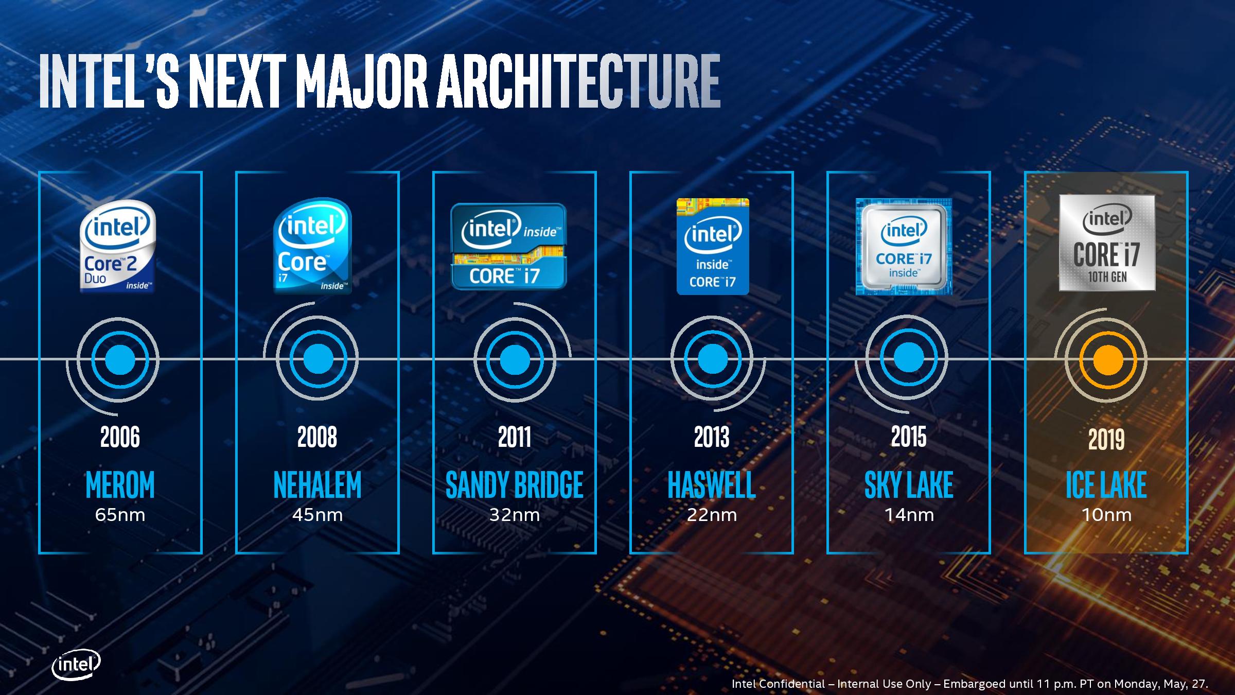
For the general user, this is a good thing™. Not only is Ice Lake set to take advantage of new process node technology, with smaller transistor and lower voltage operation, but also apply a mélange of new features and new performance benefits at the same time. It isn’t every day we see a combined ticktock from Intel (AMD has done it twice in two years), but I’m glad it is here.
If you want to find out more on the Intel 10nm process story, please read our Cannon Lake Review.
If you want to find out more on the microarchitecture behind Sunny Cove, please read our deep dive posted earlier this week. Some finer details will be discussed in this article.
The Road to Ice Lake-U and Ice Lake-Y: 11 SKUs
Today, Intel is announcing the processors for both its Ice Lake-U and Ice Lake-Y processors. These processors are now being produced in sufficient volume to supply key launch partners with hardware in order to enable laptop and mobile designs to hit the shelves by the end of the year. Intel is not currently discussing any desktop or server processor equivalents at this time: the base Ice Lake design is current a quad-core processor with HyperThreading, and a beefy integrated graphics.

Intel’s Ice Lake SoC comes in two form factors, technically called ‘Type 3’ and ‘Type 4’. Type 3 is a bigger package, suitable for 15 W-28 W Ice Lake-U designs, while Type-4 is for 9-12 W platforms under Ice Lake-Y. Out of the processors being announced today, they mostly fall into the 9 W or 15 W categories.
| Intel 10nm Ice Lake-U Series CPUs | |||||||||
| AnandTech | Cores Threads |
Base Freq |
1C Turbo |
AC Turbo |
GPU EUs |
GPU Freq |
L3 Cache |
TDP | Price 1ku |
| Core i7-1068G7 | 4 Cores 8 Threads |
2.3 | 4.1 | 3.6 | 64 | 1100 | 8 MB | 28 W | - |
| Core i7-1065G7 | 4 Cores 8 Threads |
1.3 | 3.9 | 3.5 | 64 | 1100 | 8 MB | 15 W 25 W |
$426 |
| Core i5-1035G7 | 4 Cores 8 Threads |
1.2 | 3.7 | 3.3 | 64 | 1050 | 6 MB | 15 W 25 W |
$320 |
| Core i5-1035G4 | 4 Cores 8 Threads |
1.1 | 3.7 | 3.3 | 48 | 1050 | 6 MB | 15 W 25 W |
$309 |
| Core i5-1035G1 | 4 Cores 8 Threads |
1.0 | 3.6 | 3.3 | 32 | 1050 | 6 MB | 15 W 25 W |
$297 |
| Core i3-1005G1 | 2 Cores 4 Threads |
1.2 | 3.4 | 3.4 | 32 | 900 | 4 MB | 15 W 25 W |
$281 |
Sitting at the top of the stack is the Core i7-1068G7, the sole 28W processor. The name is as follows:
- Core i7 = i7 rated
- 10 = 10th Gen Core
- 6 = Position in the Stack
- 8 = 28W
- G7 = Highest Graphics (64 EUs)
For these processors, Intel is dropping the Y and the U name, and instead putting a letter and number at the end to identify how powerful the graphics are.
The Core i7-1068G7, running at a TDP of 28 W, will be the highest performing Ice Lake processor, which Intel will reserve for premium designs by its partners. We were told that partners will get it later than the others, due to the extra validation (i.e.: binning) it requires, however it does hit the 4.1 GHz that Intel has advertised as the peak frequency of the platform. The higher TDP translates in this case to a much higher base frequency than everything else (2.3 GHz rather than 1.3 GHz), and should help with maintaining turbo frequencies when not thermally limited. This processor has Iris Plus graphics, the name Intel is giving to all Gen11 graphics parts that have 48 or more EUs (so, G4 or G7).
The rest of the U series are a nominal 15 W TDP, with base frequencies from 1.0 GHz to 1.3 GHz, and turbo frequencies up to 3.9 GHz. These processors offer a cTDP up mode of 25 W, which Intel tells us won’t actually be related to any base frequency adjustment, but it will provide a higher standard of sustained turbo frequency, depending on the OEM implementation. OEMs will have to design for 25 W in order to support it.
It is worth noting that we have three versions of the Core i5-1035, all of which differ in their graphics. The G7 version has 64 execution units, the G4 has 48 execution units, and the G1 has only 32. The G4 and G1 also go slightly lower on the CPU frequency. Both the G4 and G7 graphics will be called Iris Plus, while the G1 graphics will just be called UHD Graphics.
In order to help soak up some of the lower yielding/binning U-series parts, Intel is also going to offer a dual core Core i3-1005G1.
| Intel 10nm Ice Lake-Y Series CPUs | ||||||||
| AnandTech | Cores Threads |
Base Freq |
1C Turbo |
AC Turbo |
GPU EUs |
GPU Freq |
L3 Cache |
TDP |
| Core i7-1060G7 | 4 Cores 8 Threads |
1.0 | 3.8 | 3.4 | 64 | 1100 | 8 MB | 9 W 12 W |
| Core i5-1030G7 | 4 Cores 8 Threads |
0.8 | 3.5 | 3.2 | 64 | 1050 | 6 MB | 9 W 12 W |
| Core i5-1030G4 | 4 Cores 8 Threads |
0.7 | 3.5 | 3.2 | 48 | 1050 | 6 MB | 9 W 12 W |
| Core i3-1000G4 | 2 Cores 4 Threads |
1.1 | 3.2 | 3.2 | 48 | 900 | 4 MB | 9 W 12 W |
| Core i3-1000G1 | 2 Cores 4 Threads |
1.1 | 3.2 | 3.2 | 32 | 900 | 4 MB | 9 W 12 W |
On the Y-Series, we see a similar sort of range of i7 to i3, again with G7 down to G1. The difference here is the power envelope – the nominal TDP of these processors is 9W, however a cTDP up mode for manufacturers is available at 12W.
It is also worth looking at the processor naming for the Y-Series: the ‘m3’ naming has disappeared, and so has the letter Y. If a user didn’t know any better, these parts just look like the U-series numbers. In the name, the ‘i7-1060’, that final 0 makes all the difference.
- 0 = Y-series, ~10W (9W-12W)
- 5 = U-series, 15W (or 25W in cTDP up)
- 8 = U-series, 28W
Don’t ask what Intel would name the corresponding 35W/45W H-series processors. At this point, Intel has not discussed anything higher than 28W for consumers.
Intel's Software Development System: Tested
So as you can imagine, we (the press) have been talking with Intel for so long about Ice Lake, it is getting to a point where we’re just asking if it is ready yet. Earlier in the year, I floated an idea to Intel that basically said this:
“When you are ready with a reference design for your partners, let us test it. It’s not an optimized design, but it will have the raw performance that your partners aim to beat, and provide a good base line to drum up potential interest.”
My reference point for these discussions was what Qualcomm does on the smartphone side. For multiple generations, Qualcomm has invited select press to come test its ‘Qualcomm Reference Design’ (QRD) models for its latest smartphone chipsets. It provides a preview of the performance, and we see Qualcomm’s partners either optimize it like crazy for better performance, or produce radically unique thin form factor designs to provide the best in-hand experience while still being competitive in performance and thermals.
- The Snapdragon 855 Performance Preview: Setting the Stage for Flagship Android 2019
- The Snapdragon 845 Performance Preview: Setting the Stage for Flagship Android 2018
- The Qualcomm Snapdragon 835 Performance Preview
Well it appears that someone at Intel thought it was a good idea. The group of new employees that Intel has hired from the press side of the fence over the last year or so floated the idea up the chain, and have made it happen. We got to test Ice Lake before systems are on the shelves.
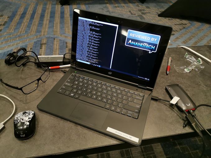
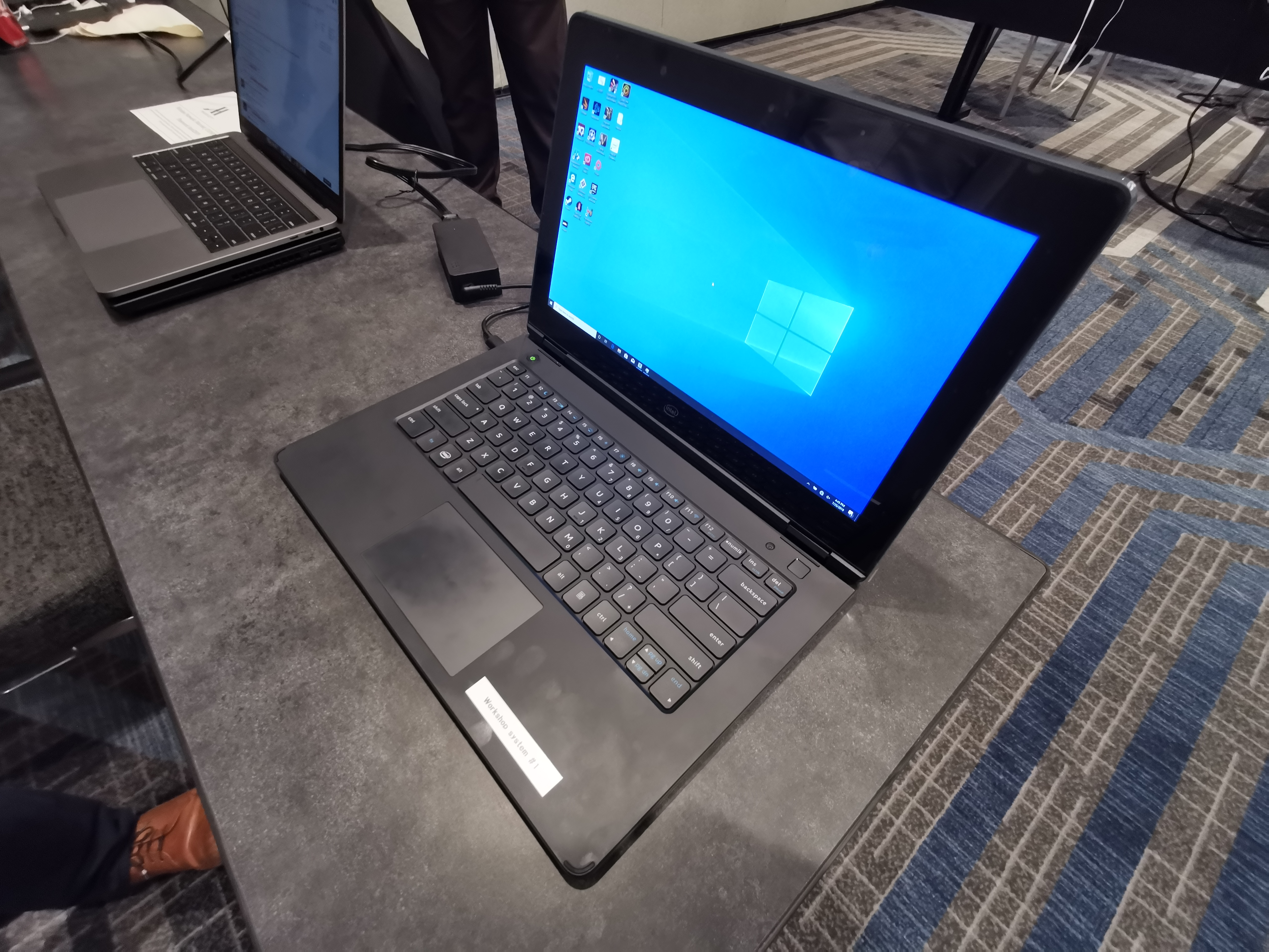
What Intel provided us was a day of testing in a conference room close to HQ in Santa Clara. These machines were Software Development Systems, or SDS laptops, that go out to Intel’s software partners like Adobe and Microsoft for functional testing.
Like other reference designs (such as Qualcomm’s), these units are designed to work, and are for the best part thermally unconstrained. The fan is on all the time, there are massive bezels, and the device itself is a bit chunky, to provide all the ports that the chip can provide. Ultimately OEMs can take these reference designs and add/remove components as they see fit, or use it as a guide to build their own from the ground up. These SDS platforms are clearly based on the Lenovo Yoga series, given the hinge mechanism and the Lenovo power bricks, but that makes sense that Intel might partner with one of its closest allies in order to produce a run of these systems.

As always with testing reference design machines, there are a few caveats worth mentioning.
- Units to stay in the room being tested (a hotel conference room near Intel HQ)
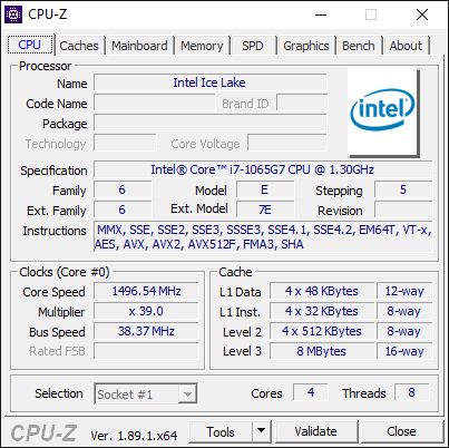
- These systems are Core i7-1065G7 units, running in 15W mode.
- Intel enabled an option so we could choose to run them in a 25W configuration.
- Intel NVMe 256GB SSD, Four Thunderbolt 3 ports, 2x4GB LPDDR4X-3733 DRAM
- The fan is on 100%
- Intel pre-installed Windows 10 Pro 1903, Build 18362.239, with ICL chipset and graphics drivers
- We were not allowed to change the OS. We could request an image reset. This was because the 15W/25W mode was a special config, plus the drivers were still beta and not wrapped in suitable installers yet
- It came with pre-installed benchmarks. We could remove these (I did).
- No thermal or battery life testing, as these units are just functional demos.
- Power testing was OK.
- Can run and install any benchmark, as long as it didn’t ‘phone home’ (to stop leaks).
- Total testing time, ~8 hours
Now to be honest, most of these from my point of view were to be expected. Only test the device in a specific location for a limited time, with no thermal/battery life on a development system. I was ok with that. Being OS limited, and having preinstalled benchmarks, was a bit awkward. I discussed this internally with other AnandTech editors, and we had differing opinions (from ‘as expected’ to ‘this could lead to cheating’).
After attending the event, to which fewer than 10 press were invited, I now understand why. Some of the press invited didn’t have OS images, didn’t bring benchmarks with them, and were quite happy to go along with the flow. Intel provided benchmarks like Geekbench and 3DMark, which those press with their audiences were happy to run. I came prepared with both a new 1903 OS image and my benchmark suite, ready to rock and roll.
What We Tested
There are two ways to approach this sort of limited time testing environment, and it was clear which of the press in attendance were going for which audience. There is device and performance testing, which aims to show how a device might perform in tests with a standard user, and there is functional testing, getting to the heart of the new microarchitecture and what it can do. We did a little of column A, but mostly column B.
Our comparison points for this test are two Huawei laptops: a Matebook 13 2019 with a Whiskey Lake i7-8565U and 8GB of DDR4-3200, and a Matebook X Pro 2018, with a Kaby Lake-R Core i7-8500U. Both of these are quad-core CPUs with a nominal TDP of 15W (the X Pro might be running in 25W mode due to its design, however). We also have dual core results from our Core i3-8121U Cannon Lake 15W laptop, a Core i3-8130U Kaby Lake-R mini-PC, and some other low powered CPUs.
| Intel Core i7-1065G7 Comparison | |||||
| Core i7-1065G7 |
AnandTech | Core i7-8565U |
Core i7-8550U |
Core i3-8130U |
Core i3-8121U |
| 10+ | Process | 14++ | 14+ | 14+ | 10 |
| Sunny Cove | uArch | Whiskey Lake | Kaby Lake-R | Kaby Lake | Cannon Lake |
| 4C / 8T | Cores | 4C / 8T | 4C / 8T | 2C / 4T | 2C / 4T |
| 1.3 GHz | Base Freq | 1.8 GHz | 1.8 GHz | 2.2 GHz | 2.2 GHz |
| 3.9 GHz | 1C Turbo | 4.6 GHz | 4.0 GHz | 3.4 GHz | 3.2 GHz |
| Gen11 | GPU uArch | Gen9.5 | Gen9.5 | Gen9.5 | - |
| 64 | GPU EUs | 24 | 24 | 24 | - |
| 1.10 GHz | GPU Freq | 1.15 GHz | 1.15 GHz | 1.00 GHz | - |
| AVX-512 | AVX | AVX2 | AVX2 | AVX2 | AVX-512 |
| 15 W | TDP | 15 W | 15 W | 15 W | 15 W |
| 2x 4GB LPDDR4X 3733 |
DRAM | 2x 4GB LPDDR3 2133 |
2x 8GB LPDDR3 2133 |
2x 4GB DDR4 2400 |
2x 4GB DDR4 2400 |
Ideally we would have tested with an AMD Ryzen 3700U in the mix as well, but unfortuantely samples of those systems seem to be rather rare. We understand that testing against AMD should be part of this analysis, but none of AMD's partners have sent us a new AMD system to test in quite a while.
With our benchmark selection, given what we wanted to test, we were actually pretty limited because a couple of our key tests actually take a number of hours. Our time breakdown started from this:
- Copy Benchmarks from USB 3.0 drive, 0h25m
- Installing benchmarks from scripts, 0h40m
- Running instruction verification tests, 0h35m
- SPEC 2006, 2h00m
- SPEC 2007, 2h20m
- Power Testing, 0h20m
That gave me 2h40m left. In that time we ran some of our regular benchmark suite, just a few tests, and then three quick game titles with our IGP settings. We tested everything at 15W, except our game tests and power tests, which we also ran in 25W mode. Unfortunately we ran out of time to do anything more.
Ideally I need another couple of days with the system. But this is what system testing is like, even with benchmarks prepared and ready to go, especially if you want to find out all the intricacies of a new architecture.
Read on for a report into our testing.


261 Comments
View All Comments
tamalero - Monday, August 5, 2019 - link
the 3d mark VRS test graph is very confusing.MASSAMKULABOX - Tuesday, August 6, 2019 - link
These chips are priced quite high esp the i3's the Dualcore is outrageous (20$ discount for half the cores and threads?).They will only sell in limited qtys at such high prices . Bring on the 14nm equiv at sane prices.what discrete gfx does the IGPU equate to? gt1030 vs 2200g vs 3400ge??
Zhentar - Tuesday, August 6, 2019 - link
The bit per cycle throughput of REP STOS is really only half of the picture - the startup latency matters a lot too! On my Skylake, I've measured a minimum latency of 29 cycles* (any REP STOS from 1 byte to 128 bytes takes 29 cycle, then it starts going up from there). Some compilers make heavy use of it even for small stores/copies (VC6, first and foremost, but also the .NET JIT for stack zeroing), so it can be pretty important to performance in some scenarios.*I am no Agner Fog... nor anywhere close to him, this measurement should be taken with a grain of salt ;-)
ballsystemlord - Wednesday, August 7, 2019 - link
@Ian
Sunny Cove SIMD chart and others have many asterisks, why?
"POPCNT Microcode 50% faster than SW (under L1-D size)"
What does this mean? The CPU uses microcode and HW, not SW, AFAIK, much less use it to implement the POPCNT instruction.
ballsystemlord - Thursday, August 8, 2019 - link
Spelling and grammar errors:Insert: I've been commenting corrections for at least 1 year now, if you guys want me to change the format, or have any request regarding phrasing, etc., just ask. Thanks for your work!
"L3 latencies look similar, however we'll dwell into that just in a bit."
I think you ment delve:
"L3 latencies look similar, however we'll delve into that just in a bit."
"IPC increases against the mobile Skylake are 33 and 38% in the integer and fp suites, though we also have to keep in d mind these figures go beyond just the Sunny Cove architecture and also include improvements through the new LPDDR4X memory controllers."
Missing percent sign and stray "d".
"IPC increases against the mobile Skylake are 33% and 38% in the integer and fp suites, though we also have to keep in mind these figures go beyond just the Sunny Cove architecture and also include improvements through the new LPDDR4X memory controllers."
"...which did not go down to well."
You mean "too" not "to":
"...which did not go down too well."
"...we actually see a number of key microarchitectural improvements bubble up through in our SPEC testing."
Excess "in":
"...we actually see a number of key microarchitectural improvements bubble up through our SPEC testing."
alysdexia - Thursday, November 28, 2019 - link
I think you mean Baalsystemlord or Bàqhàlsýstemlord.Grammar is a barbarism of ghrammatics, another word for composition or handwriting, font, format, spacing, the looks, whereas you meant diction/lecsis or register, vocabulary, declension, placement, spelling, the meaning.
you guys -> ye
nils_ - Monday, August 19, 2019 - link
I noticed on Intel Ark that Ice Lake CPUs do not have TSX instructions enabled / available. THis is interesting, since I believe TSX has also been used for some of the spectre attacks.ikjadoon - Thursday, September 12, 2019 - link
On 'Gaming Results (15W and 25W)', the graph is colored incorrectly. "On" and "Off" have the same color...and the legend colors are somehow not related to the graphic?