TSMC: 3nm EUV Development Progress Going Well, Early Customers Engaged
by Anton Shilov on July 23, 2019 3:00 PM EST- Posted in
- Semiconductors
- EUV
- TSMC
- 3nm
Development of new fabrication technologies never stops at leading-edge companies such as TSMC. Therefore, it is not surprising to hear the annoucement that development of TSMC’s 3nm node is well underway, something the company publicly confirmed last week. As it appears, the manufacturing technology is out of its pathfinding mode and TSMC has already started engaging with early customers.
“On N3, the technology development progress is going well, and we are already engaging with the early customers on the technology definition,” said C.C. Wei, CEO and co-chairman of TSMC, in a conference call with investors and financial analysts. “We expect our 3-nanometer technology to further extend our leadership position well into the future.”
Since its N3 technology is in its early stages of development, TSMC doesn't currently talk about the specific characteristics of the process nor its advantages over N5. TSMC said that it had evaluated all possible transistor structure options for 3nm and came out with ‘a very good solution’ for its clients. The specification is under development and the company is confident it would meet requirements of its leading partnering customer.
One of TSMC’s arch-rivals, Samsung Foundry, plans to use nanosheet-based Gate-All-Around MBCFET transistors for its own 3nm (3GAAE) process technology. Since TSMC will have to be competitive with its rival, we expect the company to also advance its 3nm node significantly in comparison to its 5nm node. In fact, TSMC confirms that N3 is a brand-new process technology, not an improvement or iteration of N5.
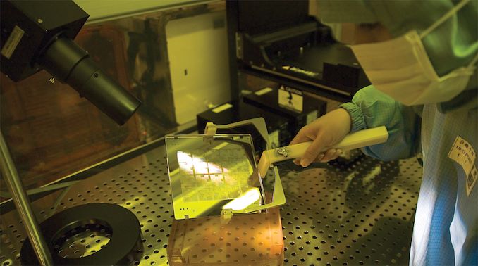
Meanwhile, it is safe to say that that TSMC’s 3 nm node will use both deep ultraviolet (DUV) and extreme ultraviolet (EUV) lithography equipment. Since TSMC’s N5 uses up to 14 EUV layers, it is likely that N3 will go even higher in the amount of layers employed. The world’s largest contract maker of semiconductors also seems to be quite happy with its EUV progress and considers the technology important for its future.
Related Reading:
- Samsung Announces 3nm GAA MBCFET PDK, Version 0.1
- TSMC’s 5nm EUV Making Progress: PDK, DRM, EDA Tools, 3rd Party IP Ready
- TSMC: First 7nm EUV Chips Taped Out, 5nm Risk Production in Q2 2019
- TSMC Details 5 nm Process Tech: Aggressive Scaling, But Thin Power and Performance Gains
- TSMC Starts to Build Fab 18: 5 nm, Volume Production in Early 2020
Source: TSMC


75 Comments
View All Comments
RSAUser - Wednesday, July 24, 2019 - link
I doubt it. Their 10nm should be doing a lot better very soon, matches 7nm TSMC, and they definitely have the money to throw at it.Wilco1 - Wednesday, July 24, 2019 - link
They are at least 1-2 years behind TSMC now, and 10nm still isn't fully working given it can only do low-end mobile chips. When you can buy 10nm 5GHz 100W desktop cores (maybe late 2020 or 2021?) you can say it finally matched 7nm TSMC.nunya112 - Wednesday, July 24, 2019 - link
I think from Intel's perspective having TSMC as a consultant for a serious fee, and possibly a % of every chip sold that is using TSMC's technology . Is pretty good business for TSMC. I guess INTEL would have to do the numbers. And a real gut check about where they actually are in their deployment of 10nm.29a - Wednesday, July 24, 2019 - link
Yes, their 10nm has been doing better very soon for a few years now.AshlayW - Wednesday, July 24, 2019 - link
Is it safe to say Intel is well and truly left behind by TSMC now? What sort of timeframe is this, will it be up against Intel "7nm" ? Does anyone have any insight in technology leadership of TSMC Vs Intel's fabs. Thanksshabby - Wednesday, July 24, 2019 - link
According to intel only 10nm is behind, 7nm is still on schedule 😂peevee - Thursday, July 25, 2019 - link
According to Intel's SJWs, 7nm is racist.Diogene7 - Friday, October 18, 2019 - link
I would say that TSMC plan to be in High Volume Manufacturing (HVM) of their 5nm node that will extensively use EUV up to 14 layers in H1 2020, and so it should be possible to purchase devices (iPhones) with a TSMC 5nm EUV chip in H2 2020.Intel plan to introduce their 7nm EUV node only in 2021, and I would think that you would be able to get your hands on a device with an Intel 7nm EUV chip in H2 2021 at best (in reality, it might even be later than that like 2022 if Intel has the same kind of struggle as for their 10nm process...).
So yes, in H2 2020, I would consider that TSMC would have at least 12 months over Intel, because devices with TSMC chip using using extensively the most advanced EUV manufacturing will be on the market while Intel wouldn’t have even start their HVM manufacturing (it takes approx. 6 months to have the 1st devices on the market after that).
melgross - Wednesday, July 24, 2019 - link
“The specification is under development and the company is confident it would meet requirements of its leading partnering customer.”Hmm, I wonder who that could be?
FunBunny2 - Wednesday, July 24, 2019 - link
At some point the fixed cost of smaller nodes will be swamped, so to speak, by the lack of demand for such density. The only way to defray fixed cost (drive down average cost, which is all the bean counters care about) is to spit out ever more widgets. Where is it going to come from?