Intel’s LGA4189-4 and LGA4189-5 for Cooper Lake & Ice Lake CPUs Now Available
by Anton Shilov on September 2, 2019 10:35 AM EST- Posted in
- CPUs
- Intel
- Ice Lake
- Xeon Scalable
- LGA4189
- Cooper Lake
TE Connectivity, a maker of various connectivity solutions, has introduced its newly-developed LGA4189 sockets for Intel’s next-generation Xeon Scalable processors supporting PCIe Gen 4. The products have been validated by Intel and are therefore ready for production of motherboards aimed at next-gen servers. It is worth noting that we already know some Cooper Lake systems are already deployed at large companies, suggesting that some LGA4189 sockets have been validated already.
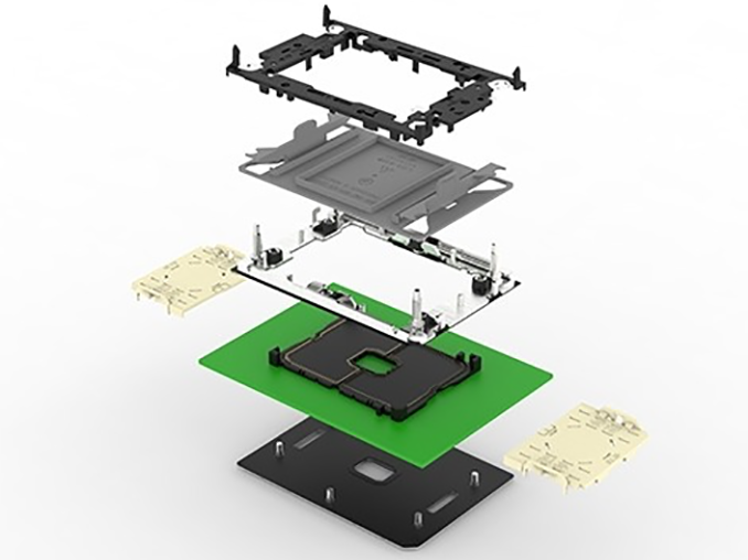
TE offers LGA4189-4 and LGA3189-5 sockets (which are called Socket P4 and Socket P5), appropriate backplates, compatible bolster plates, mounting mechanisms, and dust covers. As discovered previously, Intel’s next-generation Xeon Scalable processors in LGA4189 packaging will feature a native eight-channel memory controller and PCIe 4.0, with at least eight channel memory on standard configurations.
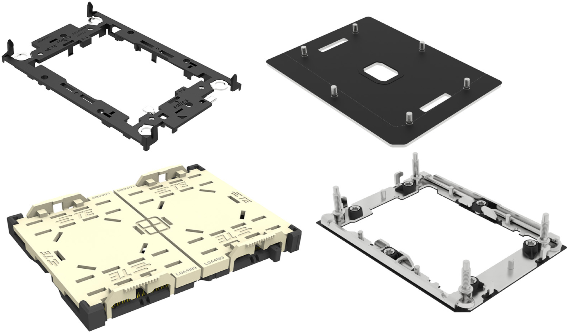
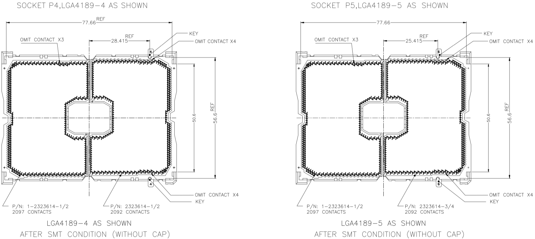
One interesting thing to note is that TE Connectivity will offer Intel’s LGA 4189 socket in two versions: the LGA4189-4 (branded as Socket P4) and the LGA4189-5 (branded as Socket P5). Being a socket maker, TE indicates that key features of Socket P4 and Socket P5 are the same: they have the same pin count, the same 0.9906 mm hex pitch, the same SP height of 2.7 mm, and the same mounting mechanisms. Meanwhile, the company does not disclose why Intel needed two separate 4189-pin sockets. Keeping in mind that Intel will have two next-generation Xeon Scalable processors — codenamed Cooper Lake and Ice Lake — it looks like that the the single-die CPUs and multi-die CPUs will use different sockets and will not be pin-to-pin compatible despite the fact that they are going to use the same platform.
A 4189-pin socket that has to provide sufficient 56-core power and support ultra-fast interconnections is extremely complex to build. TE is currently “one of the few manufacturers that can provide sockets and hardware” for Intel’s next-gen server CPUs, the company said. Meanwhile, TE says that its LGA4189 hardware is now available to interested parties, such as server makers.
Related Reading
- Power Stamp Alliance Exposes Ice Lake Xeon Details: LGA4189 and 8-Channel Memory
- Intel Xeon Update: Ice Lake and Cooper Lake Sampling, Faster Future Updates
- Intel to Offer Socketed 56-core Cooper Lake Xeon Scalable in new Socket Compatible with Ice Lake
- Intel Architecture Manual Updates: bfloat16 for Cooper Lake Xeon Scalable Only?
- Cisco Documents Shed Light on Cascade Lake, Cooper Lake, and Ice Lake for Servers
Source: TE Connectivity


31 Comments
View All Comments
JJWu - Tuesday, September 3, 2019 - link
Yes. Cooper and Ice will share a socket that is for 2S platform. For 4S platform, it will be Cooper only. LGA4189-4 and LGA4189-5 are for 2S and 4S platform separately. From Huawei's leaked roadmap, it shows that 2S and 4S platform are different.https://www.tomshardware.com/news/intel-server-ddr...
Elstar - Friday, September 6, 2019 - link
That's a useful leak! It implies that Cooper Lake is a 6-channel/6-UPI chip, and that Intel will sell a "48 core" multi-die variant of Cooper Lake for 2S configs to better compete with AMD's Epyc Rome. That being said, the multi-die setup will have only 8 of the 12 memory controllers active, which would help Intel differentiate pricing. And the 4S Cooper Lake setup will probably have more PCIe lanes than the dual-die 2S Cooper Lake setup.lefty2 - Monday, September 2, 2019 - link
> Both SKUs will are mutidie ...Yeah? Provide a link with your source.
ilt24 - Tuesday, September 3, 2019 - link
@Gondalf ... "The Ice Lake large die is 26 cores"Are you sure about that, seems odd that they would lower their core count when they are moving to a smaller process?
Elstar - Friday, September 6, 2019 - link
1) Skylake and Cascade Lake have 28 cores (6*5 mesh minus 2 for memory controllers). I'd be shocked if Cooper Lake isn't the same mesh layout.2) I've seen rumors that Ice Lake has 34 cores (6*6 mesh minus 2 for memory controllers). This seems conservative and realistic given the die shrink to 10nm. That being said, a 6*7 mesh minus 2 for memory controllers would also be reasonable given the die shrink, so either Intel has dramatically increased the core count for Ice Lake, or caches are way bigger, or they're being conservative due to yields.
In short, 26 cores seems like a typo.
quorm - Monday, September 2, 2019 - link
Are these kind of sockets with thousands of fragile pins on the motherboard ever going away? Is there really no better way to do it?ipkh - Monday, September 2, 2019 - link
The other way is to put the pins on the CPU. The mid way was slots but that won't scale to that many contacts. Guess which way is easier?And look at Threadripper mounting problems with their cartridge system.
jordanclock - Monday, September 2, 2019 - link
Well, the pins used to be on the CPU but that arrangement was swapped around because a broken pin on a motherboard is less likely to happen and almost always cheaper to replace than the CPU.If you're asking if there is some better way to physically link the CPU to the rest of the system, not that I've ever heard of. All those pins are necessary for all the links (memory, PCIe, etc.) that we expect for a modern system. We could, in theory, reduce the number of pins by making more connections serial but that's a whole different can of worms.
quorm - Monday, September 2, 2019 - link
Yeah, I'm familiar with the history and necessity for so many pins. Just wondering if there is a better mechanical alternative to make the connection. I personally have never had a problem, but I've seen several people who have.DanNeely - Monday, September 2, 2019 - link
The only alternative I know is too use thousands of solder balls instead. That gives better electrical contacts; and as a bonus means the whole 2 generations per mobo issue is avoided because swaps are impossible.