EUV Demand is Up: EUV Device Manufacturer ASML Beats Sales Estimates
by Anton Shilov on October 16, 2019 6:15 PM EST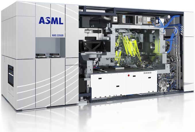
Between the smartphone revolution, cloud computing, and the Internet of Things, the demand for cutting-edge chips has never been higher. And if you have any doubts about that, then one only needs to look at the record-breaking sales of the equipment used to fab those chips. ASML, the leader in the field for photolithography, announced this week its financial results for the third quarter, revealing that its sales, profits, and net bookings all topped expectations, as the company received orders for 23 extreme ultraviolet lithography (EUVL) tools.
ASML’s revenues in Q3 2019 totaled €2.987 billion ($3.3 billion), with a net income of €627 million ($692.7 million). During the quarter, ASML sold 45 DUV and seven EUV lithography systems, as well as five used lithography systems. In total, the company sold 136 step-and-scan tools this year so far, of which 18 were EUV tools. In Q4, the company intends to ship eight EUV step-and-scan systems, bringing the total for 2019 to 30 EUV systems.
ASML’s biggest bump in the third quarter came from a total of 23 orders for Twinscan NXE EUV systems from various customers. Combined with other bookings, ASML’s net bookings totaled €5.111 billion in Q3, the company’s highest ever for a single quarter. It is particularly noteworthy that ASML reaffirmed that it expects its EUV tools to be adopted by both logic makers (i.e., CPUs, GPUs, etc.) and memory manufacturers.
As of July 2018, there were 31 EUV scanners installed at various fabs across the world, including several machines in various semiconductor research organizations. With 10 systems sold in H2 2018 and 18 EUV scanners installed this year, the number of EUV lithography tools used in the world is approaching 60 units. Of course, the number is considerably behind the number of DUV step-and-scan systems used nowadays, but it is clear that extreme ultraviolet lithography is gradually getting more widespread, and that demand is continuing to increase.
Officially, only TSMC and Samsung Foundry use ASML’s Twinscan NXE scanners to make chips using their N7+ and 7LPP manufacturing technologies. Both contract makers of semiconductors will expand their usage of EUV tools as they adopt new fabrication processes. Furthermore, Intel will use EUVL for its 7 nm technology that will be deployed across multiple fabs through 2021. Furthermore, companies like Samsung and SK Hynix are mulling the use of EUVL for DRAM production.
Here is what Peter Wennink, CEO of ASML, had to say:
“For the remainder of the year, we expect Logic to continue to be strong, driven by the leading-edge nodes supporting end-market technology and applications such as 5G and artificial intelligence. The timing of Memory recovery remains uncertain. We continue to make solid progress in EUV. Customers have introduced their first EUV manufactured devices and we have seen EUV mentioned in product announcements. In the third quarter, we shipped seven EUV systems, three of which were NXE:3400C, our higher productivity model. We received 23 EUV orders in the third quarter which contributes to our highest ever value of bookings in one quarter. This strong order flow confirms the adoption of EUV in high volume manufacturing for Logic and Memory. Our overall view for 2019 is essentially unchanged as we continue to see 2019 as a growth year.”
Related Reading:
- ASML to Ship 30 EUV Scanners in 2019: Faster EUV Tools Coming
- Samsung’s Aggressive EUV Plans: 6nm Production in H2, 5nm & 4nm On Track
- TSMC: 3nm EUV Development Progress Going Well, Early Customers Engaged
- Micron’s DRAM Update: More Capacity, Four More 10nm-Class Nodes, EUV, 64 GB DIMMs
- Samsung Completes Development of 5nm EUV Process Technology
Source: ASML


46 Comments
View All Comments
drexnx - Wednesday, October 16, 2019 - link
why sink billions into a parallel effort when ASML is amortizing that cost across every fab in the world for you?Eliadbu - Thursday, October 17, 2019 - link
Every company has it main focus, for pure-play companies they have to develop and maintain their manufacturing processes which by itself takes a lot of resources, developing and manufacturing Scanners will take unnecessary resources especially when there is working solution in the market, those companies will resort to make their own tools if there is no other available option in the market and no one intends and there is a clear need for the tool. And for price the tool would be much cheaper buying than developing and manufacturing and with such high demand it always pays itself.eldakka - Thursday, October 17, 2019 - link
"Other companies like Intel surely have the R+D money to put into this area, potentially more than ASML."In 2012 Intel invested $4.1billion into ASML for a 15% stake. AFAIK they still retain that stake. Therefore effectively they did plough $4.1billion into EUV by purchasing that stake in ASML.
Why would they want to compete with a company they are heavily invested in, and receive a share of profits from?
dropme - Thursday, October 17, 2019 - link
Intel was one of the semiconductor companies that funded ASML. And you may have to look at the development cost ASML have spent, That's a LOT of money. The EUV system itself is very expensive too.melgross - Thursday, October 17, 2019 - link
Intel, and others have investigated this. But Intel isn’t a machine design and manufacturing company. They don’t really sell machines either. The effort to produce EUV has taken a good 15 years. It’s use has been pushed out for close to a decade. Why should Intel get wrapped up in this, when it’s cheaper, and more efficient to buy it when it comes out?ksec - Thursday, October 17, 2019 - link
> I'm wondering why they haven't?Because it is business 101. Why didn't Apple buy TSMC? own the Fab, Why didn't Apple buy Qualcomm? Why Intel didn't buy AMD or Nvidia? Why should a company owns every part of their Supply Chain?
Have you consider the consequence of Intel falling to doing EUV themselves ( Cough ) while ASML did it and sell it to other Fab with higher priorities? And may even be not selling to Intel due to competitive reason.
And from 3rd part competition? There were, it was NEC, and others and they all gave up.
name99 - Thursday, October 17, 2019 - link
Semiconductor fabbing is much more than just the ASML machine.The EUV light source is from Cymer (bought by ASML, but in San Diego).
The EUV optics are from Zeiss in Germany.
The wafers used to (I'm guessing still are) from Japan, along with many of the other super-pure chemicals.
I don't know about the current (less than ideal) resists, but the newest resists are mostly being investigated by the US as far as I can tell (but I don't follow chemistry closely).
Many of the newest ideas for new transistors and how to fab them are being worked out at imec in the Netherlands.
And all these places are hiring people from all over the world.
Bottom line is: anyone stupid enough to imagine they can unilaterally take over modern fabbing (by grabbing ASML, invading Taiwan, or whatever) is going to be confronted very soon with just HOW international the whole enterprise is, and how no-one country or region has the know-how to do it all themselves.
(Each could, perhaps, build up that know-how with enough time and money, but it would not be a cheap or fast process.)
FullmetalTitan - Thursday, October 17, 2019 - link
There is so much cross-industry knowledge sharing as well. ASML scouts our engineers, we recruit people directly from the vendors, project managers move on to these R&D companies. This is constantly happening, there is a near infinite amount of knowledge on the subject that cannot be contained by one group.jvl - Friday, October 18, 2019 - link
Great insight, just minor correction: IMEC is in Belgium :-) Been to the tower, great placeArsenica - Thursday, October 17, 2019 - link
Nikon and Canon failed in developing competing EUV scanners..Regarding your second question, no large semiconductor manufacturer makes their own equipment (except for a few small scale research tools), they depend on 3rd party suppliers such as ASML, LAM research, Applied Materials, etc.