Intel's new Atom Microarchitecture: The Tremont Core in Lakefield
by Dr. Ian Cutress on October 24, 2019 1:30 PM ESTTremont: A Wider Front End and Caches
For users that have been following our analysis of the Core microarchitecture, it has been hard not to notice that Intel’s design for that family has been, among other things, to continually go wider and wider. This means more instructions in flight, larger caches, bigger buffers, bigger TLBs, more execution ports, and support for more instructions. Going wider isn’t the only thing: the microarchitecture also has to be clever, trying to maximise utilisation, as going wider does nothing for a simple stream of commands.

With Atom, going wider is a key part of the design for Tremont, but Intel has taken a couple of fundamentally different steps to manage exactly what is going on.
A Key Uplift: Fetch and Predict
Another major jump for the Atom microarchitecture are the prefetchers and branch predictors. Intel states that rather than iterate the design from Goldmont Plus, they have transplanted a large part of the prefetchers and branch predictors from the Core design on Sunny Cove. The design isn’t identical according to Intel, due to die area and power concerns, but Intel states that the principles are similar and elements like branch prediction history tables are ‘of the same order’ as the Core design.

Intel states that there is no penalty for an L1 prediction, and that the L2 prediction penalty is smaller than previous generations.
A Key Differentiator: Decode Engines
On the face of it, we have a 6-wide decode engine pared with a 4-wide allocation/dispatch engine. This is, on paper, very odd: normally we would expect the decode and dispatch to be equal in width, or at least be able to dispatch more than can be decoded in order to ensure that the re-order buffer doesn’t overflow. With the latest Core microarchitecture, called Sunny Cove, we have a 4-to-6 wide decode that also supports a micro-op cache, which all leads into a large reorder buffer and a 10-wide dispatch to the back-end. Tremont is, by contrast, has the opposite ratio.
Saying that this is a 6-wide decode engine is actually slightly incorrect. What Intel has done here is split the decode into dual 3-wide engines instead.
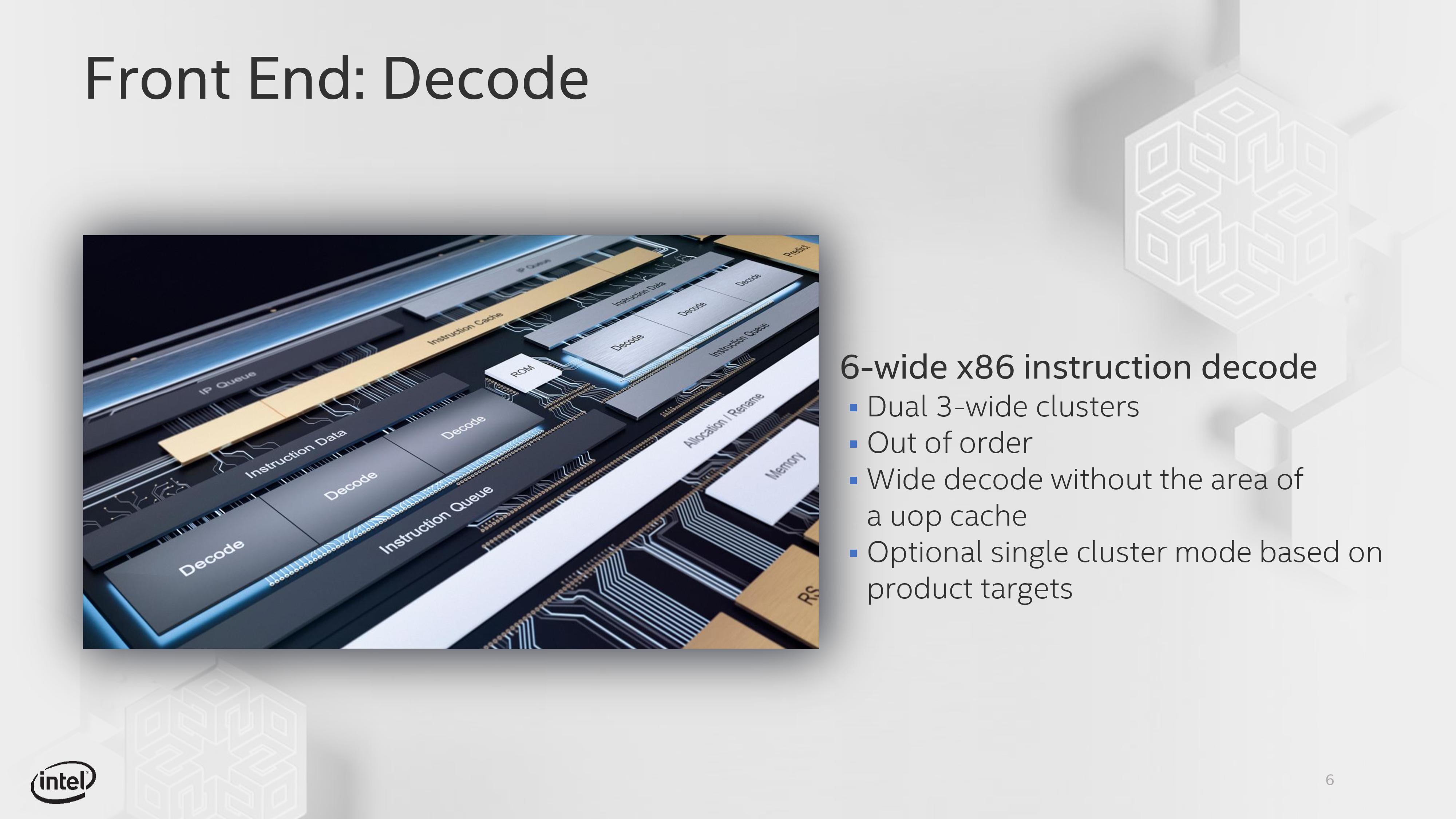
Each decode engine, when dealing with different branch predictions, can take a separate instruction stream. This allows for a higher average utilization across both of the 3-wide decode engines compared to a single 6-wide engine, but when a branch isn’t present it means that one of the decode engines can be clock gated to save power. For a single instruction stream, the Tremont design is actually only 3-wide decode, with a 4-wide dispatch.
(Technically Intel states that, through microcode, they can change the decode engines to act as a single 6-wide implementation rather than dual 3-wide engines. This won’t be configurable to the OEM, but based on demand Intel may make specific products for customers that request it.)
So just to clarify, Tremont does not have a micro-op cache. When discussing with Intel about the benefits of this dual decode engine design compared to having a micro-op cache, Intel stated that a micro-op cache can help utilize a wide-decode design better, but with a smaller per-engine decode size, they were able to see a performance uplift as well as save die area by using this dual-engine design. Intel declined to comment which one was better, but we were told that given the die size, power envelope of Atom, and the typical instruction flow of an Atom core, this design yielded the better combination of performance, power, and area.
Another improvement for Intel after the decode engines is the re-order buffer. Intel states that it can support 208 instructions, compared to 78 in Goldmont and 95 in Goldmont Plus, which is a sizeable uplift. Intel did not specify if Tremont has the ability to fuse instructions into micro-ops for the ROB (Goldmont did not), however there is a near 1:1 parity of instructions to micro-ops we were told.
Caches
Intel has also increased the size of its L1 data cache. The L1 instruction cache says at 32 KiB/core with 8-way associativity, but ever since the 22nm era, Intel has kept a 24 KiB/core L1 data cache on its Atom design. With Tremont, both the L1-I and L1-D are now a 32 KiB/core design with 8-way associativity. Intel states that its L1 data cache here has a 3-cycle latency, compared to Skylake which has a 32 KiB L1D at a 4-cycle latency, or Sunny Cove which has a 48 KiB L1D at a 5-cycle latency.
| Intel Caches | ||||||
| AnandTech | Tremont | Goldmont+ | Goldmont | Sunny Cove | Skylake | |
| Process | 10+ | 14 | 14 | 10+ | 14++ | |
| Decode | 2x3-wide | 3-wide | 3-wide | 4-6 wide | 4-5 wide | |
| Allocate | 4-wide | 4-wide | 3-wide | 10-wide | 8-wide | |
| L1 Instruction | 32 KiB/Core 8-way |
32 KiB/Core 8-way |
32 KiB/Core 8-way |
32 KiB/Core 8-way |
32 KiB/Core 8-way |
|
| L1 Data | 32 KiB/Core 8-way |
24 KiB/Core 6-way |
24 KiB/Core 6-way |
48 KiB/Core 12-way |
32 KiB/Core 8-way |
|
| L1 Latency | 3-cycle | 3-cycle | 3-cycle | 5-cycle | 4-cycle | |
| L2 Cache | 1.5-4.5 MiB Per Module 12-18 way |
1.0 MiB Per Core 16-way |
0.5-1.0 MiB Per Core 16-way |
512 KiB Per Core 8-way |
256 KiB Per Core 4-way |
|
| L2 Latency | 17-cycle | 19-cycle | 17-cycle | 13-cycle | 12 cycle | |
For the L2 cache, for most Atom cores in the past, this has essentially been a last-level cache split across all cores in a ‘module’. Depending on the generation will depend on the size of the module: for 22nm Silvermont, we saw an L2 cache of 512 KiB/core, which was increased with Goldmont up to 1.0 MB/core. With Tremont, Intel has specified that L2 will vary depending on the product, from 1.5 MiB to 4.5 MiB per module. A module for Tremont will be anything up to four cores, so we could see designs with a single core featuring 4.5 MiB of L2 cache, or a quad-core design with 1.5 MiB of L2. Within a module, all cores have access to the cache, however a core will not have access to the L2 in a different module. The L2 can be set through microcode as an inclusive or a non-inclusive cache.
Intel states that the L2 cache has an average 17-cycle latency, and the associativity will be a function of the size: 1.5 MB will be a 12-way design, while 4.5 MB will be an 18-way design. (We therefore assume that a 3.0 MB L2 will be 15-way.)
Tremont also adds support for a global L3 cache across modules. Both the L2 and L3 cache support QoS arrangements, allowing for data prioritization and memory bandwidth enforcement for specific threads or virtual machines. This is a technology that Intel introduced with Broadwell Xeons to help avoid ‘noisy neighbor’ environments in data centers.


101 Comments
View All Comments
azazel1024 - Tuesday, October 29, 2019 - link
Sure in some cases, but most not super cheap Atom implementations from even the Cherry Trail era weren't all on the USB2 bus, at least not the eMMC. Most typical performance I saw was >100MB/sec reads and 30 or so MB/sec writes on slower implementations. Some of the better eMMC implementations were hitting ~180MB/sec reads and 70MB/sec writes and 6-7k IOPS.Not SSD performance, but storage performance isn't the issue with HEVC playback. HEVC support is. My Cherry Trail doesn't support H265 decode. I can play back a 1080p HEVC file, but the processor is running between 70-90% utilized when doing it. For an H264 encoded 1080p file it typically runs about 15% utilization to do it.
It can't handle 4k decode.
My biggest issue has been networking performance on the one that I have. Some are better setup, but not all of them. My first generation Cherry was an Asus T100. Max storage performance was 110MB/sec reads, 37MB/sec writes, 5k IOPS. The microSD card slot maxed out at 20MB/sec read and writes. The Wireless was 1:1 802.11n and maxed at about 10MB/sec down and 8MB/sec up (obviously not concurrently) and it was only 40MHz on 5GHz, not 2.4GHz (20MHz only on that).
My current one is a T100ha after my T100 died. Some improvements, some backslides. The read/write speed is up to 170MB/sec and 48MB/sec with 7k max IOPS. The microSD card reader can hit about 80MB/sec reads and 30MB/sec writes (in a card reader in my desktop the same microSD card can hit 80MB/sec reads and 50MB/sec writes). The wireless though is WAY slower. It hits 6MB/sec down and 3MB/sec up max. Supposedly it can do the same 40MHz on 5GHz and 20MHz on 2.4GHz, but I don't see anything like real 1:1 40MHz performance on 5GHz (which should be in the ballpark of 10-12MB/sec, 80-100Mbps).
That is honestly my biggest complaint is the wireless on it is just horrendous. I often use an 802.11ac nano dongle in the keyboard dock USB3 port as that easily pushes 20MB/sec up and down. Even simple website loading using it is significantly faster than the embedded wireless. I know it is a cheap tablet/2-in-1, but it is one of those probably springing an extra $1-2 on BOM for a nicer even 802.11n 1:1 solution would have gone a long way. Let alone at the time it was released, 1:1 802.11ac wireless options were pretty widely available.
I am curious if someone like Asus (or someone else, I am NOT tied to them) will use Tremont in any small 2-in-1. Heck, an update to Surface with one might be nice. I do like the smaller form factor of a 10-11" size tablet. I almost always use my 2-in-1 as a laptop, so a hard keyboard dock is reasonably important to me (but a really nice type cover would be fine, I almost always use it on a table, not on my lap), but I do sometimes use it as an actual tablet for reading (movie/TV/YouTube would generally be fine as a laptop as I am rarely just holding my tablet in front of my face to do that. Usually on a table/desk, occasionally sitting on my knees/stomach but docked). I don't need a TON of performance with one. But at the same time, if I want to grab a movie off my server for an overnight trip or something, it is kind of painful to be downloading a 3GB file at 6MB/sec and having to wait the better part of 10 minutes to download the darn thing. It is usually worth my while to go rummage in my desk drawer, grab my USB3 GbE adapter, plug it in to my tablet and in to a spare LAN drop in one of my rooms and quick grab the file at ~50MB/sec or so a second of the micro SD card write speed and be done in maybe 2 minutes of doing all those steps and the download time. Let alone if I want to grab maybe 2 or 3 movie files at 6-10GB.
A nicer screen would of course be real swell too, but honestly 720p on a 10.1" screen isn't horrible. The wireless limitations are my biggest headache. A bit more CPU and GPU performance would also be nice. I wouldn't mind being able to handle slightly newer/more advanced games on it, but frankly it isn't my gaming machine nor do I need it to be. Portable is more important to me that powerful. But some of the basic tasks it needs to be better at/feeling its age.
Wireless being at least 2x better, and it would be nicer to be more like 3-4x better (which 802.11ac 1:1, if you don't mess up the implementation IS at ~20-25MB/sec). If CPU performance was maybe 15-20% better (and Tremont sounds like it is probably more like 50-100% faster than Cherry trail), GPU maybe twice as fast (also sounds like it would be a lot faster than that), storage performance and peripheral storage is fine as it is on my T100ha, but yeah I sure as heck don't mind some improvements there also. Battery life being better would be nice, but I usually manage >10hrs if I am not doing anything super intensive. I could even live with the current screen, though better coverage of sRGB (I think mine is about 70% sRGB), contrast (actually mine is pretty good at I think around 800:1 or so, not great, but not bad) and higher resolution (900p would be nice, 1080p better).
Maybe someone can do all that in a package less than $400. Oh and 8GB of RAM and 128GB of storage. Max $500 price tag.
eek2121 - Monday, October 28, 2019 - link
eMMC isn't typically known for speed.Namisecond - Friday, November 1, 2019 - link
Most eMMC isn't optimized for performance. They tend to be optimized for cost.levizx - Friday, October 25, 2019 - link
You are confusing iGPU with QSV, they are different IP blocks.solidsnake1298 - Monday, October 28, 2019 - link
I am not confusing QSV with the iGPU. While QSV is functionally different from the EUs that generate "graphics" and physically occupies a different section of die area from the EUs, QSV is LOGICALLY part of the "iGPU." I'm not sure this is an option in my particular BIOS, but humor me here. If I were to disable the iGPU in my J4205 and use an add-in Nvidia/AMD GPU wouldn't that also mean that QSV is no longer available? On the full power desktop side, if I bought a KF SKU Intel processor (the ones without an iGPU), doesn't that mean that QSV is not available?Yes, I was referring to QSV specifically. But QSV is a feature of Intel's iGPUs. Just like NVENC is a feature of most of Nvidia's GPUs.
abufrejoval - Tuesday, November 5, 2019 - link
If you disabled the iGPU, the VPU is gone, too. But you don't need to disable the iGPU when you add a dGPU: Just connect your monitor to the dGPU and leave the iGPU in idle.Not sure it's worth it, though. I can't see that the Intel VPUs are any better than the ones from Nvidia or AMD, neither in speed nor in quality. And for encoding quality/density CPU still seems best, if most expensive in terms of energy.
solidsnake1298 - Tuesday, November 5, 2019 - link
The point of my post was to point out that I was not "confusing" QSV with the iGPU when they are logically part of the same block on the die. You can't have QSV (Quick Sync Video) without the iGPU being active. So when, in the context of video decoding, I refer to "iGPU" I am obviously talking about the QSV block on the iGPU.Namisecond - Friday, November 1, 2019 - link
4K output was completely dependent upon the vendor to implement. I have a Gemini Lake laptop that used an HDMI 1.3 or 1.4 output chip. I love it for it's all-day long battery and don't miss the 4K output at all.hyno111 - Thursday, October 24, 2019 - link
Atom performance actually improved a lot every generation. I would perfer Goldmont Plus based Pentium than the low power dual core Skylake++ without turbo.Samus - Thursday, October 24, 2019 - link
That's not true. Atom at various stages has actually taken a step BACKWARDS in performance.Most obviously, Cedarview was around 20% slower per product SKU than Pineview, thought performance per watt remained nearly identical. Still, the D525 remained the top performaning Atom for years until Avoton launched in 2013.
Atom was also plagued with x64 compatibility issues until Avoton officially supported the x86 extension, along with virtualization, mostly because Avoton was designed specifically as a "Server" product, finding its way in everything from NAS to SMB microservers where it performed terribly compared to even rudimentary RISC CPU's.
It's an absolute marketting failure by Intel to continue pushing the cute name Atom with the reputation they have built for it. They were moving away for awhile, branding many traditional Atom-architecture products Pentium J\Celeron J, then going back on that move to shift Pentium\Celeron back to the Core microarchitecture, and further mutilating the process by actually calling Core-based CPU's Atom's with the x3/x5/x7.
No wonder AMD has maintained consistent OEM support. At least their CPU product stack has made sense for the last 10 years...