Intel's new Atom Microarchitecture: The Tremont Core in Lakefield
by Dr. Ian Cutress on October 24, 2019 1:30 PM ESTTremont: A Wider Front End and Caches
For users that have been following our analysis of the Core microarchitecture, it has been hard not to notice that Intel’s design for that family has been, among other things, to continually go wider and wider. This means more instructions in flight, larger caches, bigger buffers, bigger TLBs, more execution ports, and support for more instructions. Going wider isn’t the only thing: the microarchitecture also has to be clever, trying to maximise utilisation, as going wider does nothing for a simple stream of commands.

With Atom, going wider is a key part of the design for Tremont, but Intel has taken a couple of fundamentally different steps to manage exactly what is going on.
A Key Uplift: Fetch and Predict
Another major jump for the Atom microarchitecture are the prefetchers and branch predictors. Intel states that rather than iterate the design from Goldmont Plus, they have transplanted a large part of the prefetchers and branch predictors from the Core design on Sunny Cove. The design isn’t identical according to Intel, due to die area and power concerns, but Intel states that the principles are similar and elements like branch prediction history tables are ‘of the same order’ as the Core design.

Intel states that there is no penalty for an L1 prediction, and that the L2 prediction penalty is smaller than previous generations.
A Key Differentiator: Decode Engines
On the face of it, we have a 6-wide decode engine pared with a 4-wide allocation/dispatch engine. This is, on paper, very odd: normally we would expect the decode and dispatch to be equal in width, or at least be able to dispatch more than can be decoded in order to ensure that the re-order buffer doesn’t overflow. With the latest Core microarchitecture, called Sunny Cove, we have a 4-to-6 wide decode that also supports a micro-op cache, which all leads into a large reorder buffer and a 10-wide dispatch to the back-end. Tremont is, by contrast, has the opposite ratio.
Saying that this is a 6-wide decode engine is actually slightly incorrect. What Intel has done here is split the decode into dual 3-wide engines instead.
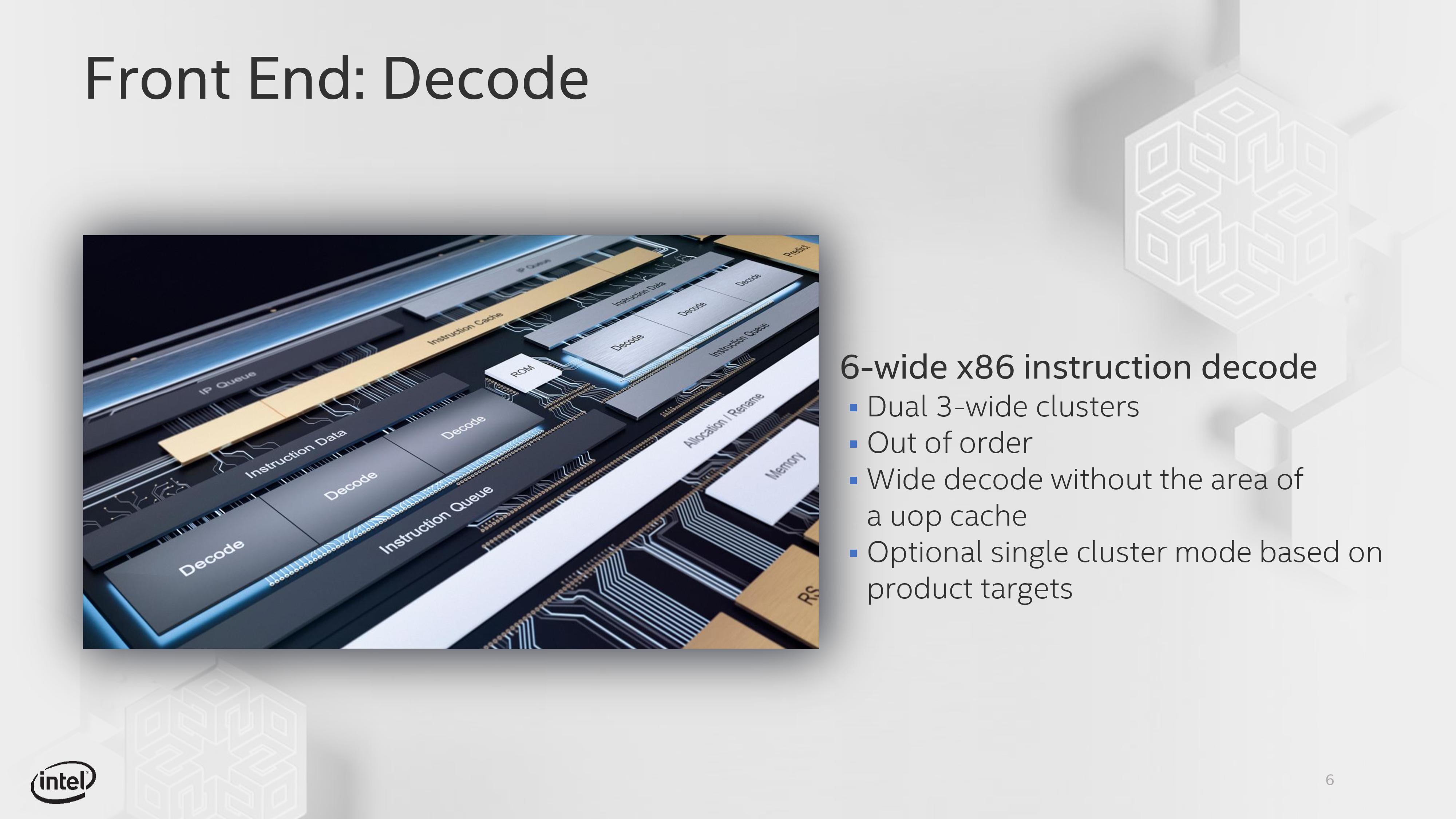
Each decode engine, when dealing with different branch predictions, can take a separate instruction stream. This allows for a higher average utilization across both of the 3-wide decode engines compared to a single 6-wide engine, but when a branch isn’t present it means that one of the decode engines can be clock gated to save power. For a single instruction stream, the Tremont design is actually only 3-wide decode, with a 4-wide dispatch.
(Technically Intel states that, through microcode, they can change the decode engines to act as a single 6-wide implementation rather than dual 3-wide engines. This won’t be configurable to the OEM, but based on demand Intel may make specific products for customers that request it.)
So just to clarify, Tremont does not have a micro-op cache. When discussing with Intel about the benefits of this dual decode engine design compared to having a micro-op cache, Intel stated that a micro-op cache can help utilize a wide-decode design better, but with a smaller per-engine decode size, they were able to see a performance uplift as well as save die area by using this dual-engine design. Intel declined to comment which one was better, but we were told that given the die size, power envelope of Atom, and the typical instruction flow of an Atom core, this design yielded the better combination of performance, power, and area.
Another improvement for Intel after the decode engines is the re-order buffer. Intel states that it can support 208 instructions, compared to 78 in Goldmont and 95 in Goldmont Plus, which is a sizeable uplift. Intel did not specify if Tremont has the ability to fuse instructions into micro-ops for the ROB (Goldmont did not), however there is a near 1:1 parity of instructions to micro-ops we were told.
Caches
Intel has also increased the size of its L1 data cache. The L1 instruction cache says at 32 KiB/core with 8-way associativity, but ever since the 22nm era, Intel has kept a 24 KiB/core L1 data cache on its Atom design. With Tremont, both the L1-I and L1-D are now a 32 KiB/core design with 8-way associativity. Intel states that its L1 data cache here has a 3-cycle latency, compared to Skylake which has a 32 KiB L1D at a 4-cycle latency, or Sunny Cove which has a 48 KiB L1D at a 5-cycle latency.
| Intel Caches | ||||||
| AnandTech | Tremont | Goldmont+ | Goldmont | Sunny Cove | Skylake | |
| Process | 10+ | 14 | 14 | 10+ | 14++ | |
| Decode | 2x3-wide | 3-wide | 3-wide | 4-6 wide | 4-5 wide | |
| Allocate | 4-wide | 4-wide | 3-wide | 10-wide | 8-wide | |
| L1 Instruction | 32 KiB/Core 8-way |
32 KiB/Core 8-way |
32 KiB/Core 8-way |
32 KiB/Core 8-way |
32 KiB/Core 8-way |
|
| L1 Data | 32 KiB/Core 8-way |
24 KiB/Core 6-way |
24 KiB/Core 6-way |
48 KiB/Core 12-way |
32 KiB/Core 8-way |
|
| L1 Latency | 3-cycle | 3-cycle | 3-cycle | 5-cycle | 4-cycle | |
| L2 Cache | 1.5-4.5 MiB Per Module 12-18 way |
1.0 MiB Per Core 16-way |
0.5-1.0 MiB Per Core 16-way |
512 KiB Per Core 8-way |
256 KiB Per Core 4-way |
|
| L2 Latency | 17-cycle | 19-cycle | 17-cycle | 13-cycle | 12 cycle | |
For the L2 cache, for most Atom cores in the past, this has essentially been a last-level cache split across all cores in a ‘module’. Depending on the generation will depend on the size of the module: for 22nm Silvermont, we saw an L2 cache of 512 KiB/core, which was increased with Goldmont up to 1.0 MB/core. With Tremont, Intel has specified that L2 will vary depending on the product, from 1.5 MiB to 4.5 MiB per module. A module for Tremont will be anything up to four cores, so we could see designs with a single core featuring 4.5 MiB of L2 cache, or a quad-core design with 1.5 MiB of L2. Within a module, all cores have access to the cache, however a core will not have access to the L2 in a different module. The L2 can be set through microcode as an inclusive or a non-inclusive cache.
Intel states that the L2 cache has an average 17-cycle latency, and the associativity will be a function of the size: 1.5 MB will be a 12-way design, while 4.5 MB will be an 18-way design. (We therefore assume that a 3.0 MB L2 will be 15-way.)
Tremont also adds support for a global L3 cache across modules. Both the L2 and L3 cache support QoS arrangements, allowing for data prioritization and memory bandwidth enforcement for specific threads or virtual machines. This is a technology that Intel introduced with Broadwell Xeons to help avoid ‘noisy neighbor’ environments in data centers.


101 Comments
View All Comments
Valantar - Friday, October 25, 2019 - link
Intel doesn't use the Atom name any longer, at least not officially. Is it anywhere in this slide deck? As for Pentium/Celeron, P/C Silver is Atom-based, Gold is Core, and that applies even to the newest product stack (Intel even launched updated Goldmont Plus Gemini Lake Pentium/Celeron chips just a few days ago, topping out with the J5040 and N5030: https://www.techpowerup.com/260374/intel-gemini-la... Confusing? Absolutely. But nothing has changed since the (admittedly stupid) gold/silver branding was introduced.levizx - Sunday, October 27, 2019 - link
Maybe get your eyes checked? This while article is about the Tremont uArch, so are the slides.Gemini Lake is old news, doesn't matter what "new" product Intel releases. Intel had Atom on their roadmap as late as last December.
BUT, their May investor meeting failed to disclose what brands Lakefield will be under. So as far as the general public know. Atom is still alive in ultra low-power Server SoC and embedded SoC space.
eddman - Sunday, October 27, 2019 - link
There hasn't been an atom branded mainstream (desktop, laptop or tablet) processor strarting with goldmont; only server, embedded and automotive parts, and starting with goldmont plus there is none whatsoever.eddman - Sunday, October 27, 2019 - link
*No edit function*What I meant to say is, while atom branding is not dead, intel has moved away from using it for the products facing the mainstream consumers. It's all pentium and celeron.
I doubt they'd bring it back for lakefield, which even uses a single "big" sunny cove core.
eek2121 - Monday, October 28, 2019 - link
Not true, Apollo Lake showed up in an SBC form factor. That is goldmont + gen9 iGPU.eek2121 - Monday, October 28, 2019 - link
Gah anandtech needs to join the year 2000 and add an edit button. The atom CPU I have seen used is the atom e3900. Yes it is technically an embedded part, but it is also used by consumers for various projects, including home theater applications and the like.eddman - Monday, October 28, 2019 - link
Such devices are not mainstream.Namisecond - Friday, November 1, 2019 - link
You're talking the uarch. The person you're talking to is talking about the Atom brand name.rrinker - Thursday, October 24, 2019 - link
Depends on what you use them for. I have a box I built at least 7 years ago, so whatever Atom was current - I think it was the first one to have 2 cores. I ran Linux on it, mostly for controlling my model railroad. It was plenty fast enough, even with a slow hard drive and just 2GB RAM. I couldn't stream video to it, but music was fine, and it ran both the control program as well as a 2D CAD program to design track plans.Not every task a computer does requires insane speeds. There's a whole lot more than just gaming.
1_rick - Thursday, October 24, 2019 - link
They're good enough for things like NASes.