Intel's new Atom Microarchitecture: The Tremont Core in Lakefield
by Dr. Ian Cutress on October 24, 2019 1:30 PM ESTTremont: A Wider Front End and Caches
For users that have been following our analysis of the Core microarchitecture, it has been hard not to notice that Intel’s design for that family has been, among other things, to continually go wider and wider. This means more instructions in flight, larger caches, bigger buffers, bigger TLBs, more execution ports, and support for more instructions. Going wider isn’t the only thing: the microarchitecture also has to be clever, trying to maximise utilisation, as going wider does nothing for a simple stream of commands.

With Atom, going wider is a key part of the design for Tremont, but Intel has taken a couple of fundamentally different steps to manage exactly what is going on.
A Key Uplift: Fetch and Predict
Another major jump for the Atom microarchitecture are the prefetchers and branch predictors. Intel states that rather than iterate the design from Goldmont Plus, they have transplanted a large part of the prefetchers and branch predictors from the Core design on Sunny Cove. The design isn’t identical according to Intel, due to die area and power concerns, but Intel states that the principles are similar and elements like branch prediction history tables are ‘of the same order’ as the Core design.

Intel states that there is no penalty for an L1 prediction, and that the L2 prediction penalty is smaller than previous generations.
A Key Differentiator: Decode Engines
On the face of it, we have a 6-wide decode engine pared with a 4-wide allocation/dispatch engine. This is, on paper, very odd: normally we would expect the decode and dispatch to be equal in width, or at least be able to dispatch more than can be decoded in order to ensure that the re-order buffer doesn’t overflow. With the latest Core microarchitecture, called Sunny Cove, we have a 4-to-6 wide decode that also supports a micro-op cache, which all leads into a large reorder buffer and a 10-wide dispatch to the back-end. Tremont is, by contrast, has the opposite ratio.
Saying that this is a 6-wide decode engine is actually slightly incorrect. What Intel has done here is split the decode into dual 3-wide engines instead.
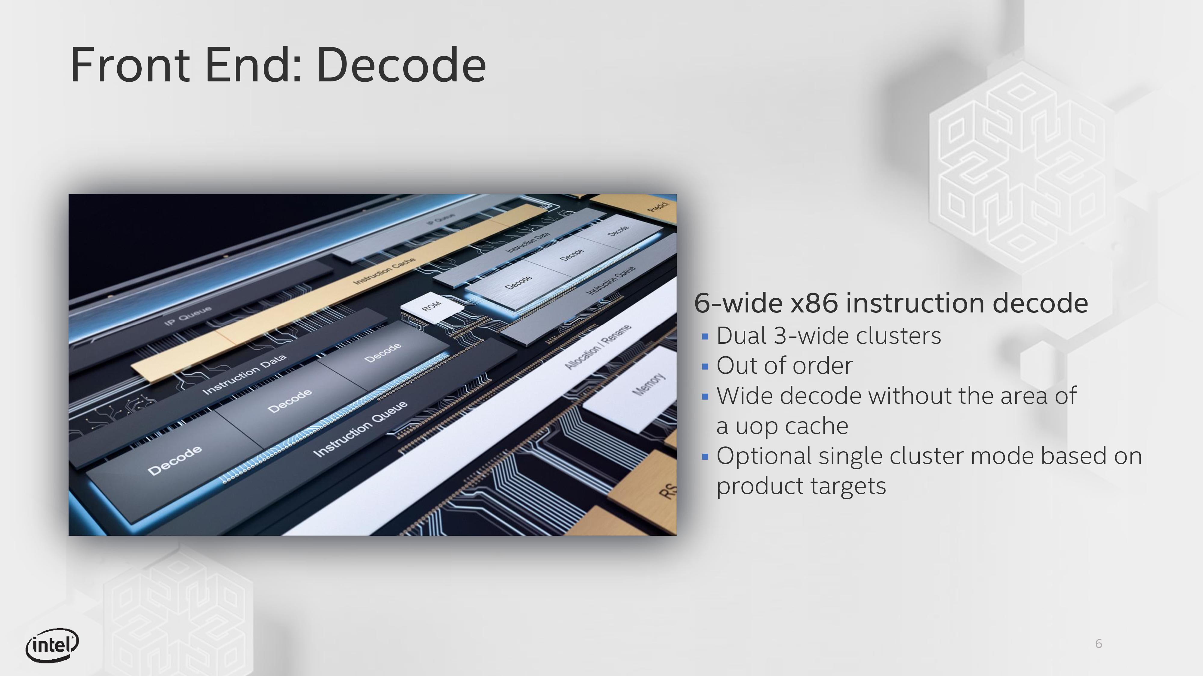
Each decode engine, when dealing with different branch predictions, can take a separate instruction stream. This allows for a higher average utilization across both of the 3-wide decode engines compared to a single 6-wide engine, but when a branch isn’t present it means that one of the decode engines can be clock gated to save power. For a single instruction stream, the Tremont design is actually only 3-wide decode, with a 4-wide dispatch.
(Technically Intel states that, through microcode, they can change the decode engines to act as a single 6-wide implementation rather than dual 3-wide engines. This won’t be configurable to the OEM, but based on demand Intel may make specific products for customers that request it.)
So just to clarify, Tremont does not have a micro-op cache. When discussing with Intel about the benefits of this dual decode engine design compared to having a micro-op cache, Intel stated that a micro-op cache can help utilize a wide-decode design better, but with a smaller per-engine decode size, they were able to see a performance uplift as well as save die area by using this dual-engine design. Intel declined to comment which one was better, but we were told that given the die size, power envelope of Atom, and the typical instruction flow of an Atom core, this design yielded the better combination of performance, power, and area.
Another improvement for Intel after the decode engines is the re-order buffer. Intel states that it can support 208 instructions, compared to 78 in Goldmont and 95 in Goldmont Plus, which is a sizeable uplift. Intel did not specify if Tremont has the ability to fuse instructions into micro-ops for the ROB (Goldmont did not), however there is a near 1:1 parity of instructions to micro-ops we were told.
Caches
Intel has also increased the size of its L1 data cache. The L1 instruction cache says at 32 KiB/core with 8-way associativity, but ever since the 22nm era, Intel has kept a 24 KiB/core L1 data cache on its Atom design. With Tremont, both the L1-I and L1-D are now a 32 KiB/core design with 8-way associativity. Intel states that its L1 data cache here has a 3-cycle latency, compared to Skylake which has a 32 KiB L1D at a 4-cycle latency, or Sunny Cove which has a 48 KiB L1D at a 5-cycle latency.
| Intel Caches | ||||||
| AnandTech | Tremont | Goldmont+ | Goldmont | Sunny Cove | Skylake | |
| Process | 10+ | 14 | 14 | 10+ | 14++ | |
| Decode | 2x3-wide | 3-wide | 3-wide | 4-6 wide | 4-5 wide | |
| Allocate | 4-wide | 4-wide | 3-wide | 10-wide | 8-wide | |
| L1 Instruction | 32 KiB/Core 8-way |
32 KiB/Core 8-way |
32 KiB/Core 8-way |
32 KiB/Core 8-way |
32 KiB/Core 8-way |
|
| L1 Data | 32 KiB/Core 8-way |
24 KiB/Core 6-way |
24 KiB/Core 6-way |
48 KiB/Core 12-way |
32 KiB/Core 8-way |
|
| L1 Latency | 3-cycle | 3-cycle | 3-cycle | 5-cycle | 4-cycle | |
| L2 Cache | 1.5-4.5 MiB Per Module 12-18 way |
1.0 MiB Per Core 16-way |
0.5-1.0 MiB Per Core 16-way |
512 KiB Per Core 8-way |
256 KiB Per Core 4-way |
|
| L2 Latency | 17-cycle | 19-cycle | 17-cycle | 13-cycle | 12 cycle | |
For the L2 cache, for most Atom cores in the past, this has essentially been a last-level cache split across all cores in a ‘module’. Depending on the generation will depend on the size of the module: for 22nm Silvermont, we saw an L2 cache of 512 KiB/core, which was increased with Goldmont up to 1.0 MB/core. With Tremont, Intel has specified that L2 will vary depending on the product, from 1.5 MiB to 4.5 MiB per module. A module for Tremont will be anything up to four cores, so we could see designs with a single core featuring 4.5 MiB of L2 cache, or a quad-core design with 1.5 MiB of L2. Within a module, all cores have access to the cache, however a core will not have access to the L2 in a different module. The L2 can be set through microcode as an inclusive or a non-inclusive cache.
Intel states that the L2 cache has an average 17-cycle latency, and the associativity will be a function of the size: 1.5 MB will be a 12-way design, while 4.5 MB will be an 18-way design. (We therefore assume that a 3.0 MB L2 will be 15-way.)
Tremont also adds support for a global L3 cache across modules. Both the L2 and L3 cache support QoS arrangements, allowing for data prioritization and memory bandwidth enforcement for specific threads or virtual machines. This is a technology that Intel introduced with Broadwell Xeons to help avoid ‘noisy neighbor’ environments in data centers.


101 Comments
View All Comments
mode_13h - Saturday, October 26, 2019 - link
Yes, fadd is simply floating-point add. Same for fmul.What makes FMA "fused" is that the product isn't truncated before the accumulate, resulting in higher precision. So, what's "fused" is the multiplication and accumulation.
Fused-add or fused-multiply makes no sense - they each only do one thing, so what would you even be fusing?
The Hardcard - Thursday, October 24, 2019 - link
when I squint at the power/performance graph, I don’t see much of a power savings for Tremont. If that is 1.5 for Sunny, it looks like Tremont is will be more like 1 watt rather than 200mW. is it my eyes or are they being loose with the graph. also, it looks like performance drops much faster than power.Lakefield seems like it should be 2+4 rather than 1+4. it will be interesting to see how it compares to the 8cx for performance and battery life.
Santoval - Thursday, October 24, 2019 - link
In the graph Sunny Cove goes down to 12 - 13% "relative power" while Tremont reaches around 4 - 5%. So, if we assume a lowest of 13% relative power for Sunny Cove at 1.5W and a lowest of 4% for Tremont, this would suggest that Sunny Cove at its lowest power/frequency consumes 3.25 (13/4) times more power than Tremont at its lowest power/frequency.If that's indeed the case, and that graph is accurate, then Tremont consumes ~0.45 watts (1.5W / 3.25) at its lowest power, not 1 watt. However if that graph is only slightly inaccurate Tremont might really go down to 200mW operation mode. For instance if Sunny Cove's relative power was meant to terminate at 20% and Tremont's at 3% then their difference in power consumption at the lowest power mode is (20/3) 6.67 times, thus Tremont would go down to ~220mW.
The Hardcard - Thursday, October 24, 2019 - link
interesting, we both put Sunny at 12 percent. But my eyes put Tremont at 8 percent, which is how I got one watt. It just looks much closer to the 10 than the one. But, I assume Microsoft got figures that made sense to them so maybe you’re right.name99 - Friday, October 25, 2019 - link
We have to look at why this product exists. To me it looks like IBM's 8-way threading, ie a product of the decadent stage of CPU design, when the primary impulse becomes to game the markets rather than to optimize engineering metrics.Look at the performance/energy curve. There is SO MUCH overlap with Core. That makes little sense for a big.LITTLE type system -- if the primary goal is low power, you optimize the one core for low power, the other for performance, and make little effort to extend the low power performance beyond the lowest the high power core goes. (You want a small amount of overlap for hysteresis but not much more.) If you look at Apple's cores (which I know best) this is clear; the small cores max at about 30% of the performance of the large cores, and the large cores can clock down to about 1/3 maximum frequency.
But what if your goal is NOT primarily energy saving? The Tremont presentation talks a whole lot about performance, little (nothing that I saw) about where they saved energy and how much. What if your goal is to create a "reasonably powerful" lower end core, to at least good enough match current ARM AND to be able to expand your provision of multi-core (for PCs) and many-core (for laptops) without having to give up those nice juicy Core profits?...
Clearly you can think of Tremont as an A75 equivalent, to be sold to designs thinking of jumping ship at that performance level. But you can also view it as Intel's way of providing low-end laptops/desktops with 5 (or 6? who knows what the SMT situation of the large core is) threads without having to drop the prices on i5s. Likewise a way to compete with those 48 and 64-core lightweight ARMs (ThunderX, Cavium and suchlike) while again not having to drop the price of the large Xeons.
In this light, the omission of decent AVX is not a bug, it's a feature; it's one more reason that these are low class cores meant for peasants, while decent people should continue to pay for Cores.
On financial grounds, this may make sense, and Intels' plan is presumably to add AVX-512 when SVE becomes too common too ignore (but not until then...)
On strategic grounds does it make sense? Hmm.
- It may just prevent even more people from ever bothering to design, compile, and optimize for AVX. Maybe likewise for persistent memory? (That support seems pretty fragmented, and I'm sure Tremont won't help.)
- Even Intel isn't so large that they can keep creating substantially improved new designs every year (something that's become very clear over the past few years).
This particular fork seems to be one that doesn't allow for that much learning across the two teams (and may even lead to deliberate crippling if the Tremont direction gets "too" good).
Of course other design houses are even more opaque than Intel (I don't think we have any idea how much cross-learning there is between the ARM big and little core teams. Apple certainly APPEARS to have very good cross-learning [both the lock-step feature support and the very low performance overlap as minor pieces of evidence] but who can be sure?)
But they seem to have a better aligned set of incentives to keep everyone happy and in sync. (Team A goes for performance at this power level, team B for performance up to X and no further and this lower power level.)
Whereas Intel seems to be in the difficult situation (that VERY WIDE performance overlap range between the two cores) of "yeah, keep making it faster, but not too fast --- you'll know when you're too fast because we'll crush your spirit at that point..."
Anyway, lots of rambling here, but I think the key insight is to NOT see this as an ENERGY big.LITTLE play, regardless of what Intel says, but as a way to provide more cores at the low-end without hurting Core prices. (Of course there is still that pesky damn AMD forcing high-end Xeon prices to halve... Well, one battle at a time.)
Namisecond - Friday, November 1, 2019 - link
8cx will probably beat Lakefield in terms of efficiency, but Lakefield has native x86 and probably better perceived performance.azfacea - Thursday, October 24, 2019 - link
wrong title. this aint new. its pentium 4 shrink/rebrandJorgp2 - Thursday, October 24, 2019 - link
Lol, norozquilla - Thursday, October 24, 2019 - link
I love my J5005 (Gemini Lake) as an HTPC, and I lent it to a relative for a while after his AMD A10-7860K (Piledriver, meh...) failed, he felt it worked around the same, and faster on videos...Which is why I love this CPU, it is fanless and stays at around ~8W and plays back 10bit 4K content in my living room TV without any issues. I also added a CNVI 802.11ac module, it performs great.
Hopefully this Tremont Core will provide something like that, but I will upgrade until there is AV1 hardware decoding. With which GPU will it be paired, a Gen11 something? I think AV1 is still a bit down the road with x86, ARM already has a couple of proposals.
For day to day office and HTPC duties, I haven't found a better alternative (maybe RPi4 in this segment?), I'm also waiting to see the Ryzen embedded alternatives for home use, so far only expensive industrial-ish options.
GreenReaper - Thursday, October 24, 2019 - link
Usually the video block is shared across all segments, so if the APU form of Navi picks up AV1 support, chances are it'll be available. Might be a while until truly low-end APUs are available, though.