Intel’s Manufacturing Roadmap from 2019 to 2029: Back Porting, 7nm, 5nm, 3nm, 2nm, and 1.4 nm
by Dr. Ian Cutress on December 11, 2019 3:00 PM EST
Update: After some emailing back and forth, we can confirm that the slide that Intel's partner ASML presented at the IEDM conference is actually an altered version of what Intel presented for the September 2019 source. ASML added animations to the slide such that the bottom row of dates correspond to specific nodes, however at the time we didn't spot these animations (neither did it seem did the rest of the press). It should be noted that the correlation that ASML made to exact node names isn't so much a stretch of the imagination to piece together, however it has been requested that we also add the original Intel slide to provide context to what Intel is saying compared to what was presented by ASML. Some of the wording in the article has changed to reflect this. Our analysis is still relevant.
One of the interesting disclosures here at the IEEE International Electron Devices Meeting (IEDM) has been around new and upcoming process node technologies. Almost every session so far this week has covered 7nm, 5nm, and 3nm processes (as the industry calls them). What we didn’t expect to see disclosed was an extended roadmap of Intel’s upcoming manufacturing processes. It should be noted that the slide presented at the conference by Intel's partner, ASML, was modified slightly from its original source.
They say a slide is worth 1000 words. Here’s 1000 words on Intel's future.
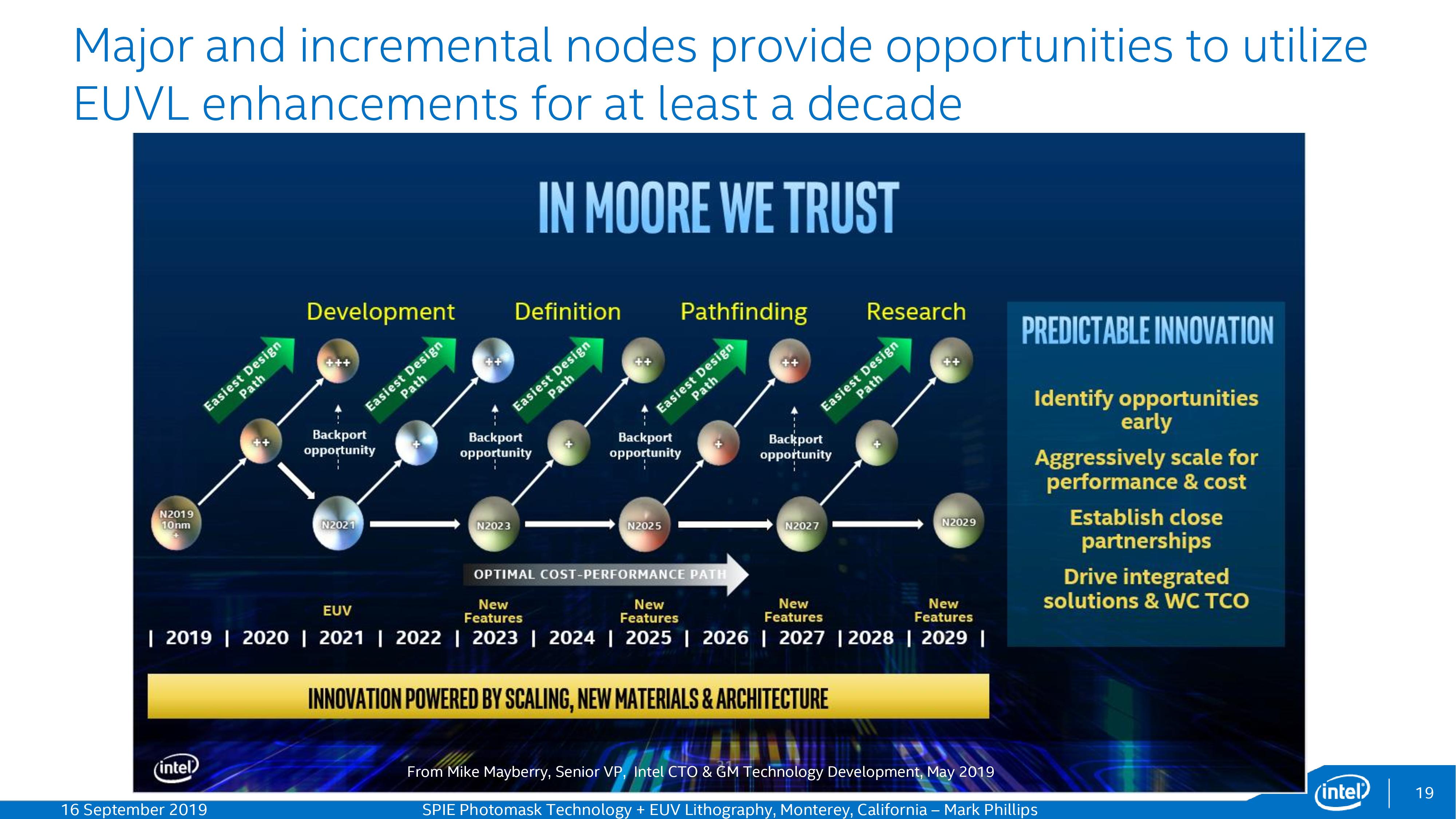
Intel's slide, as presented in September
This is Intel's original slide, not detailing which nodes in which years. However, it should be easy enough to figure out that each one of the elements in the bottom row is the next process node along, otherwise the +/++ wouldn't make sense.
ASML applied these assumptions to the slide it presented at the IEDM keynote, but the company did not disclose that they had modified the slide.
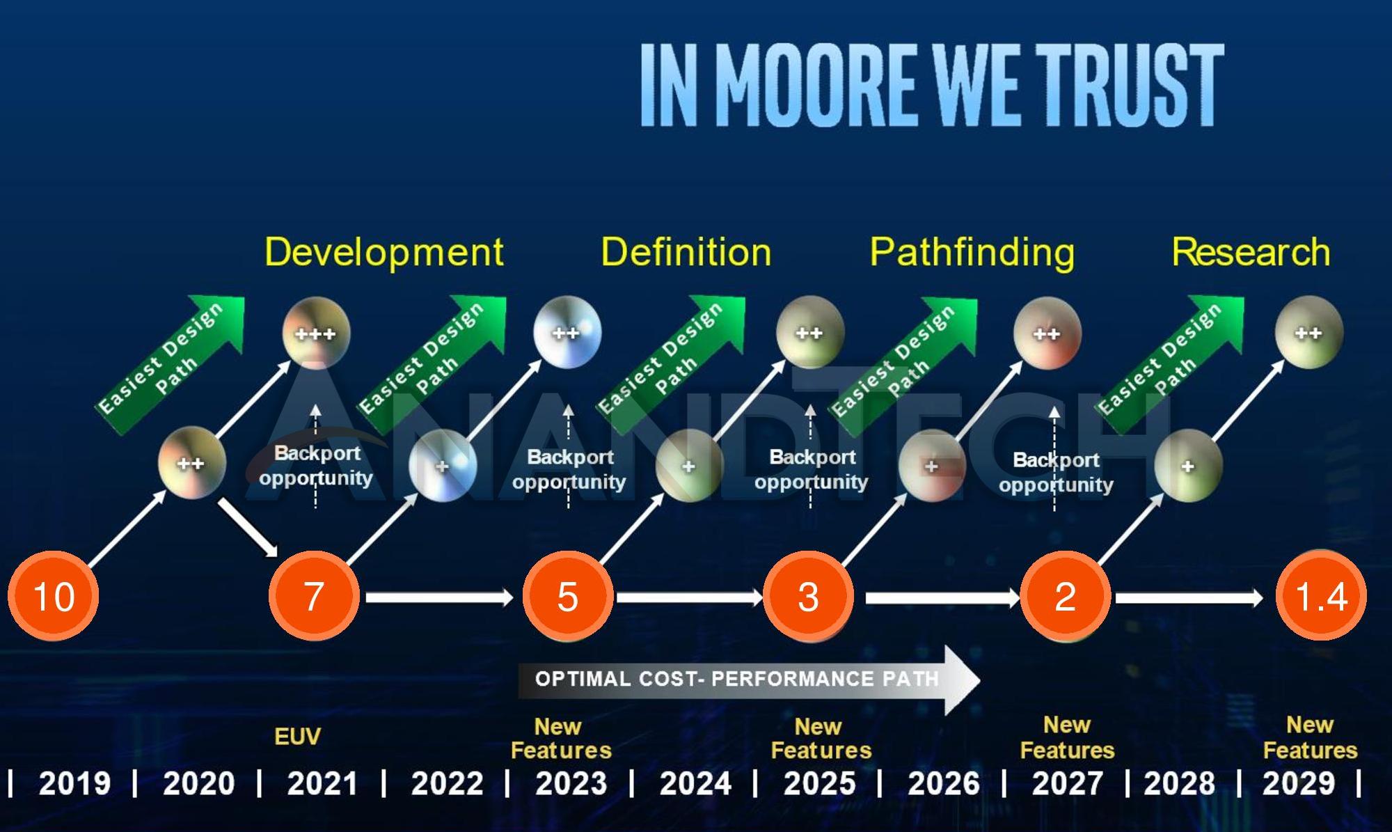
Intel's slide with ASML's animations overlayed, as shown in the slide deck distributed by ASML
So let’s go through some key areas.
1.4nm in 2029
Intel expects to be on 2 year cadence with its manufacturing process node technology, starting with 10nm in 2019 and moving to 7nm EUV in 2021, then a fundamental new node in each of 2023, 2025, 2027, 2029. This final node is what ASML has dubbed '1.4nm'. This is the first mention on 1.4nm in the context of Intel on any Intel-related slide. For context, if that 1.4nm is indicative of any actual feature, would be the equivalent of 12 silicon atoms across.
It is perhaps worth noting that some of the talks at this year’s IEDM features dimensions on the order of 0.3nm with what are called ‘2D self-assembly’ materials, so something this low isn’t unheard of, but it is unheard of in silicon. Obviously there are many issues going that small that Intel (and its partners) will have to overcome.
+, ++, and Back Porting
In between each process node, as Intel has stated before, there will be iterative + and ++ versions of each in order to extract performance from each process node. The only exception to this is 10nm, which is already on 10+, so we will see 10++ and 10+++ in 2020 and 2021 respectively. Intel believes they can do this on a yearly cadence, but also have overlapping teams to ensure that one full process node can overlap with another.
The interesting element to these slides is the mention of back porting. This is the ability for a chip to be designed with one process node in mind, but perhaps due to delays, can be remade on an older ‘++’ version of a process node in the same timeframe. Despite Intel stating that they are disaggregating chip design from process node technology, at some point there has to be a commitment to a process node in order to start the layouts in silicon. At that point the process node procedure is kind of locked, especially when it goes to mask creation.
In the slide, it shows that Intel is going to allow a workflow such that any first gen 7nm design could be back ported to 10+++, any first gen 5nm design could be back ported to 7++, and so on. One can argue that this roadmap might not be so strict with the dates – we have seen Intel’s 10nm take a long time to bake, so expecting the company to move with a yearly cadence on + updates alongside a two-year cadence with main process technology nodes would appear to be a very optimistic and aggressive cadence strategy.
Note that this isn’t the first mention of back porting hardware designs when it comes to Intel. With the current delays to Intel’s 10nm process technology, it has been widely rumoured that some of Intel’s future CPU microarchitecture designs, originally designed with 10nm (or 10+, 10++) in mind might actually find a home on a 14nm process due to the success of that process node.
Development and Research
Normally with process node developments, there will be different teams working on each process node. This slide states that Intel is currently in development of its 10+++ optimizations as well as the 7nm family. The idea is that the ‘+’ updates are capturing the low hanging fruit from a design standpoint every generation, and the number represents a full node benefit. Interestingly we see Intel’s 7nm being based on 10++, whereas in the future Intel sees 5nm come from the base 7nm design, and 3nm coming from 5nm. There is no doubt that some of the optimizations that enter each +/++ update will filter into future designs as and when they are needed.
In this slide, we have Intel’s 2023 node currently in the definition stage. At this IEDM conference there’s a lot of talk about 5nm in this timeframe, so some of those improvements (such as manufacturing, materials, consistency, etc.) will ultimately end up in Intel’s process depending on which design houses they partner with (historically Applied Materials). It is worth noting that 5nm is listed as a 2023 node, which is around the time that ASML will start selling its ‘High NA’ EUV machines to help with better path definition during the manufacturing process. I’m not sure if High NA will intercept at 5nm or 3nm, assuming this Intel roadmap has its dates correct and Intel is able to stick to it, but it is something to consider
Beyond 2023, Intel is currently in the ‘path-finding’ and 'research' mode. As always when looking this far out, Intel is considering new materials, new transistor designs, and such. At this IEDM conference we’re seeing a lot of talk of gate-all-around transistors, either as nano-sheets or nano-wires, so no doubt we’re going to see some of that as FinFET runs out of steam. TSMC is still using FinFETs for its 5nm process (Intel’s 7nm equivalent), so I wouldn’t be surprised if we see something like nano-sheets then nano-wires (or even hybrid designs) come into Intel’s manufacturing stack.
It’s worth also pointing out, based on the title of this slide, that Intel still believes in Moore’s Law. Just don’t ask how much it’ll cost.


138 Comments
View All Comments
BurntMyBacon - Wednesday, December 11, 2019 - link
IIRC from my ASIC layout days, the advertised node number used to be the smallest drawn channel length in the minimum sized transistor. However, given that a transistor is more than just a gate, the size of a transistor is necessarily larger than the channel. It is also not square in dimensions and the ratio of length to width can vary (particularly when different gate types like finFET vs Gate All Around are used). So calculating the difference in number of transistors per given area is not as simple as the calculations put forth.The level of consistency eroded a bit when the nodes label started corresponding to the smallest feature size (usually a DRAM cell feature) which up until recently loosely corresponded to about half the drawn channel length and varies between manufacturer.
Finally, the level of consistency was entirely lost when manufacturers started using node labels as marketing terms that no longer correspond to any particular feature size. Even within the same manufacturer on the same general node (lets say 7nm) the actual feature sizes can vary depending on which particular 7nm process you are using.
That all said, the nodes that have historically been targeted are generally targeted to produce roughly 2x the transistors in the same area. This doesn't always work out perfectly, particularly when the layout of the transistor changes to incorporate different gate types, but this is an example of letting Moore's Law drive the target.
So that was a fairly long winded way of saying I expect the 64x will be closer to the truth. That said, I believe that you are correct in your assertion that they should be using decimal places for nodes. This is likely marketing at work. Probably the reason they used 1.4nm was not any target feature size, but because it is 1/10 of 14nm and that looks good in marketing.
FreckledTrout - Wednesday, December 11, 2019 - link
Since FinFet you are right the node names don't really mean much. Frankly they should be naming them by actually transistor densities but even then it can be bs.Adonisds - Wednesday, December 11, 2019 - link
Since 14nm to 10nm is 2.7 scaling, a better projection would be 86x densityCiccioB - Thursday, December 12, 2019 - link
No.There's not a 10->14nm with 2.7x density gain.
Intel tried, but failed.
ksec - Tuesday, December 10, 2019 - link
Well 3nm's cost model is pretty much done if we are talking about TSMC. And it is not expensive from Apple, Huawei, Qualcomm perspective. Remember AWS, and now possibly Google and Microsoft are in the game as well. So Cost will not amortised with more players on board. High NA EUV should be required for 2nm, along with GAA that could double the price of 3nm again. ( For now it seems TSMC has decided 3nm wont be GAA, compared to Samsung rushing for GAA first )Then there is 1.4nm. I believe it is here or Sub 1nm that we will see Moore's law being extended to 3 years instead of the current cadence.
haukionkannel - Wednesday, December 11, 2019 - link
Semember that TSMC 7nm is actyally 40-50nm... and same as Intel 10nm... The marketing nm Are getting really far out from reality in all manufacturers! What 1.4nm marketing means in reality? 30-40nm?Sure Intel, Samsung, and TSMC can go smaller, but in reality They Are now at 40-50nm... so the Atom level is not so near in reality.
name99 - Wednesday, December 11, 2019 - link
Rather than complain about whose node name is or is not correct, remember that what matters is- TSMC is shipping products that achieve the promised 100MTR/mm^2 on 7nm
- Intel is (barely) shipping products that achieve half their promised 100MTR/mm^2 on their 10nm
But your point about “operating at atom scale” is valid and needs to be said, repeatedly.
back2future - Friday, December 13, 2019 - link
Wouldn't it be more useful then defining transistor density on comparable volume?https://arstechnica.com/information-technology/201...
https://cdn.arstechnica.net/wp-content/uploads/201...
AnGe85 - Thursday, December 19, 2019 - link
That's nonsense. N7 and P1274 are both using approx. 100 MTr/mm2 with their high density Libs, and Intel is shipping and products are already in the market (additionally to 10nm FPGAs).And these libs are only used for special use cases. For example AMDs Zen2-Chiplet only utilizes about 53 MTr/mm2 with their high perf design and it is therefore far away from the upper process limit, which should be no surprise, because AMD already has enough problems reaching high frequencies (which additionally is no surprise because of the shrinked node and smaller structures.)
Korguz - Friday, December 20, 2019 - link
but.. yet.. they are still very competive with intels high frequency cpus... point is ??intels 10nm process.. isnt available on more then 4 cores.. and cant hit high frequencies..