I Ran Off with Intel’s Tiger Lake Wafer. Who Wants a Die Shot?
by Dr. Ian Cutress on January 13, 2020 9:00 AM EST- Posted in
- CPUs
- Intel
- Trade Shows
- Tiger Lake
- 10+
- CES 2020

One of the surprises at CES from Intel was the presence of Tiger Lake, Intel’s next generation platform beyond Ice Lake. Tiger Lake is Intel’s vehicle for delivering the first generation of its Xe-LP graphics in a mobile form factor, and there has been a lot of buzz around what Tiger Lake exactly is. We learned this week that it is built on a 10nm+ process, which is different to the ‘10nm’ Ice Lake process (and don’t ask about what Cannon Lake was). Intel has also promoted that Tiger Lake will have higher performance than Ice Lake, both in CPU and graphics, and come with the next generation AI features. Tiger Lake will be out by the end of 2020, but the thing that surprised us most at CES 2020 was the presence of a Tiger Lake wafer.
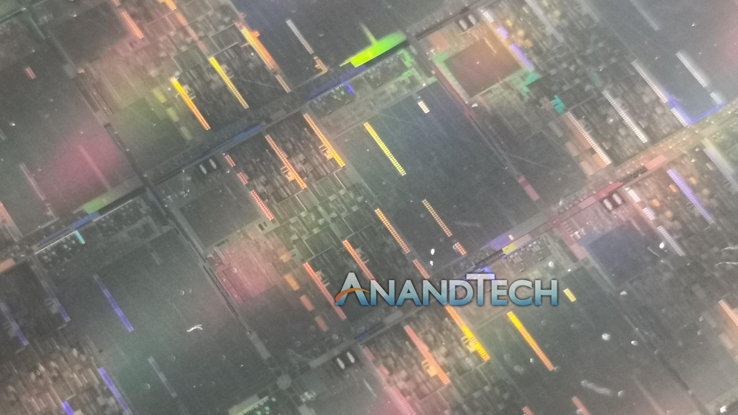
With a wafer, we can do a few things. With the right angle, we can determine how many die there are on the wafer, and by correlation, the die size. Here’s a good photo taken of the wafer, which we can count the die horizontally and vertically.

In this photo, we can count the die at the widest points of the 300mm wafer. Very rarely to ‘exact numbers of die’ on a wafer, because the reticle is moved to maximize the number of whole die. This is the case here, as we see at the edges ‘half’ die. But for the purposes of die size calculations, we have to take those into account. By sheer luck, in both the x and y dimensions, the two die on the edges come to almost exactly a whole die. This gives us dimensions of 22 die in one direction and 28 die in the other, or 13.64 mm by 10.71 mm, creating a die size of around 146.1 mm2.
| Die Sizes | |||||
| AnandTech | x | y | Die Size | Cores | EUs/ CUs |
| AMD Zen 2 Chiplet | 10.32 | 7.34 | 75.75 mm2 | 8 | - |
| Intel Ice Lake | 11.44 | 10.71 | 122.52 mm2 | 4 | 64 |
| Intel Tiger Lake | 13.64 | 10.71 | 146.10 mm2 | 4 | 96 |
| AMD Picasso | 19.21 | 10.92 | 209.78 mm2 | 4 | 11 |
| AMD Renoir | By eye, I said 150 mm2. I was almost right. Precise numbers coming in an article tomorrow... :) |
||||
Calculating die size is relatively easy in this regard. Actually getting a die shot showing features of the silicon is much harder. Luckily, I spend enough time with the wafer to get that as well.
Click through for a higher resolution image
There are the obvious structures – in the middle we have four cores, on the left is some of the IO logic, on the top right is the Thunderbolt part of the silicon, and on the main right hand side is the Xe graphics.
Current leaks point to Tiger Lake being a quad-core CPU with 96 execution units. Now we know already from Intel’s disclosures that an Xe graphics unit is different to a Gen graphics unit, with an Xe unit capable of doing SIMT work (working on data on its own) individually or SIMD work (wider vector units) collectively by switching modes through software. We confirmed through Raja Koduri that there is no physical difference between the SIMT and SIMD units, and that they operate in this way.
So the quad core we can confirm. For the GPU section, can we actually see 96 execution units? Well, with this first image, I can theroretically see more, however, as we go through the motions, the assumptions are flawed based on this single image alone.
Now this image is hard to make out, but it looks like an Xe unit on its own is very small. It’s very easy to count how many units we have in the top row: 8. In order to reach 96, we would then need to count 12 in the other dimension, however that dimension doesn’t seem to split into 12 evenly. It’s very faint, but we can see that an Xe execution unit is actually quite thin. The effect is easily seen in the top right corner and the bottom right corner, but you can clearly see a unit being thinner in this dimension. How many units do we have in this dimension exactly? I can count 30. It’s fairly easy to see the first five, slightly hardware for the next 5, and then extrapolating that distance down to the end is an effective 3x, making this full GPU block consist of 8x30 units. That makes 240 units.
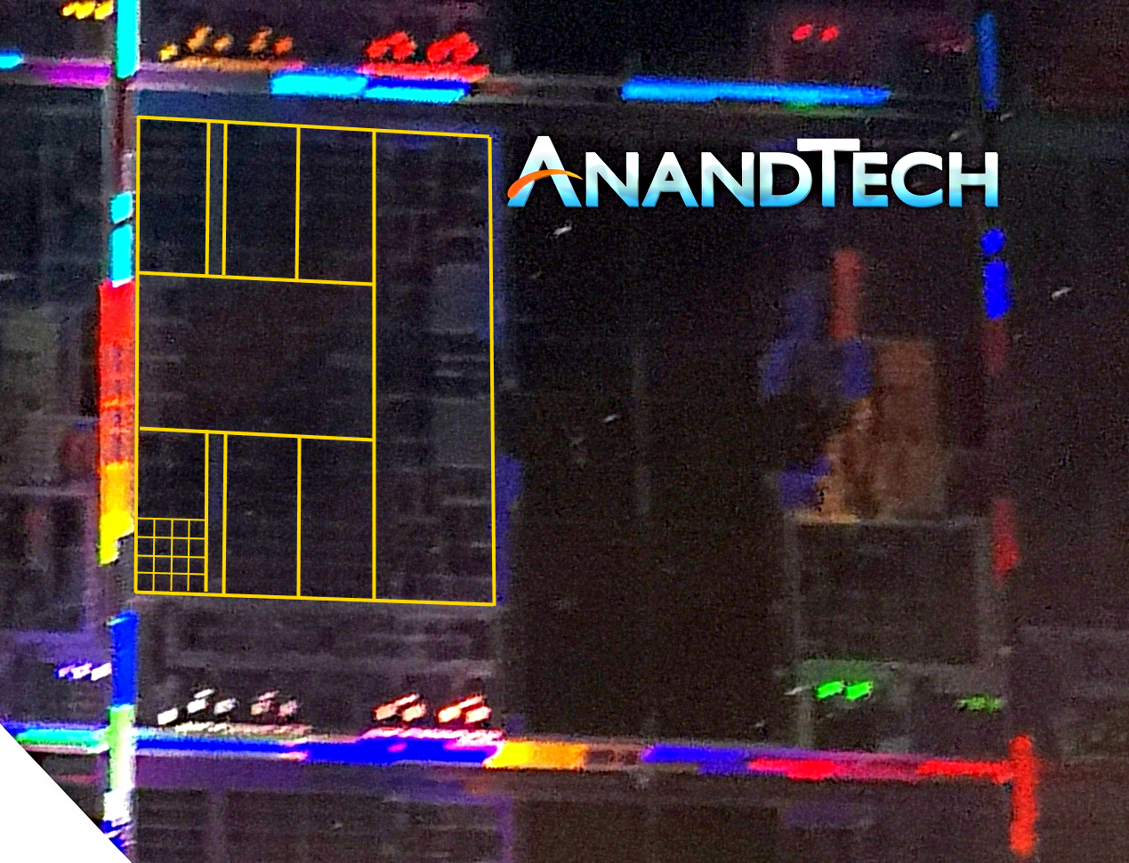
However, this assumes that the block is just a regular array of execution units. We know this not to be the case. Through additional photos, I noticed that the graphics block had a lot of structure, and it isn’t just a regular array.

Click through for a higher resolution
So in this diagram, and based what we know about Ice Lake, is that the GPU is split 75:25 into compute and media silicon. So we can make out three distinct blocks of 4x4 units on each side (which gives a total of 4x4x6 = 96 EUs), then followed by what looks like a 3x2 unit, which is likely to be some sort of cache.In the middle is a big block of larger units, and then on the top side of this image, the media section, looks like a bit of a mess.
So this is a case of the GPU having 96 EUs by design.
GPU on the left
In the Gen graphics, each execution unit was actually formed of hardware that had seven threads per unit, and as a result a 64 execution unit integrated graphics chip actually had access 448 threads for work. When we compare to say AMD’s APUs, they use 8-11 compute units (CUs) depending on the product. Each one of these compute units are actually 64 streaming processors (SPs) working in tandem on collective data, and 10 CUs = 640 SPs. It will be interesting to see what Intel has done with the design here – it looked as if during Intel’s HPC DevCon late last year that a standard execution unit has eight threads this time. But considering we’re seeing a range of structures within the silicon, it’s clear that Intel has done something significantly different with the design of the Xe graphics execution unit.
So here you have it. Here’s what we know about Intel’s Tiger Lake CPU:
- Four Cores, Likely updates to the Sunny Cove microarchitecture found in Ice Lake (Willow Cove?)
- Xe-LP Graphics, 96 EUs confirmed
- 146.1 mm2 die size
- 10+ nm process node (non-EUV)
- Enhanced DL-Boost Support (AVX-512, VNNI, Xe Graphics, GNA 2.0)
- Thunderbolt 4 Support

Here’s another prediction to make: I think that Intel is making Tiger Lake its volume 10nm-class product. As we’ve seen from Ice Lake, while partners can run it in 15 W or 25 W mode, Intel hasn’t yet launched its 28W TDP variant, let alone one that goes up to 45 W for the H-series CPUs (the Core 10th Gen H-series that Intel launched at CES were only 14++ Comet Lake). Now Ice Lake can turbo quite high, up to 50+ W power as we’ve seen in our testing, but that still means that each of the cores are scaling from 2 W to 12 W, and for a desktop product it really needs to go up to 20W or even more – Intel seems to be hitting the frequency efficiency cliff with Ice Lake quite early, suggesting that it’s unlikely that we will see desktop processors based on Ice Lake. Server processors, with 20-50 cores under 200W, only need to hit 10 W per core, making sense in that market (yields permitting).
If Intel can get that frequency efficiency curve under control for Tiger Lake, then Tiger Lake will nominally be the 10nm desktop product we’ve been waiting for. However, that also puts it on target for a 2021 launch. Intel hasn’t stated if the silicon we’ve seen is aimed at the 15 W market or something higher, however with only four cores, one would assume it would be that ultra-thin laptop market rather than a primary desktop CPU.

Intel also had a PCB with a Tiger Lake CPU on board. It should be noted that the CPU shown is using Intel's Type 4 packaging, which has historically been used with its Y-series processors. Despite this, Intel stated on stage at CES, and in the press releases, that this was a U-series part. This either means that we will see Type 4 packaging going up to 15 W, or it was a mislabel. We're wating to hear back from Intel.
The CPU is paired with the chipset, in order to give the IO support, in a single package. There are few things to make out here, such as the DRAM, what looks like a modem, and the Thunderbolt 4 Type-C ports at the end. This is the board that goes into Intel’s Horseshoe Bend concept 17-inch foldable laptop.

As you can see, this is an all-screen laptop with a foldable display, showcasing the Tiger Lake hardware. This is just a prototype, for Intel’s partners to form the basis of future designs on – it was quite thick and heavy for regular intents and purposes, but the idea is that if you need to use a wireless keyboard, it can fit in the nook between the two halves of the display when it is folded up. The prototype also had a stand embedded into the rear, so the laptop can act as a full 17-inch display when rotated.
Intel has confirmed that Tiger Lake will be shipping this year. Exactly into what with whom we don’t know yet, although we expect to see Ice Lake systems being upgraded with Tiger Lake and its Xe graphics.
I don’t think Intel will let me run off with wafers ever again.
#ontherun #TigerLake pic.twitter.com/Dhm1TwlcjV
— Dr. Wafer Eater ✈️ #CES2020 (@IanCutress) January 8, 2020


107 Comments
View All Comments
maroon1 - Monday, January 13, 2020 - link
96 EU should easily beat AMD low power APU even without even counting the architecture that Xe brings. Also, Tiger lake is rumored to use LPDDR5 memoryI feel like Tiger lake will beat AMD new APU in GPU and per core performance. While AMD APU is going to win in multi-core performance (intel IPC advantage and higher clocks will not be enough to offset the 8 core advantage that AMD have)
AMD new APU focus more CPU performance than GPU. THey are using 512 vega cores which is less than today APU, but clock speed will be higher. It will be slightly faster than current APU in GPU performance.
Gondalf - Monday, January 13, 2020 - link
Honestly i can't see Renoir H beating actual Coffee Lake cpu line in commanding a discrete GPU. Without a steady turbo clock speed you can't do much.So basically AMD is in a segment of the market with not so high GPU needs and some multithread desires without much performance in single thread. I don't know if they will penetrate much in Intel mobile dominium.
Pretty strange choice.
arashi - Monday, January 13, 2020 - link
2020 product vs 2021 product.Go back into your cave Gondaft.
alufan - Monday, January 13, 2020 - link
just lol so AMD has an 8 core 7nm chip with a newer GPU coming in the form of a new Navi implementation lets see how they stack up, in the meantime we can buy AMDs current product that beats intels current product, when exactly will this be on the shelf?like I always say competitive products benefit us all however predicting a product thats probably at least 6-7 months as a minimum off release is the best and therefore the world is blue ....well thats just daft
phoenix_rizzen - Monday, January 13, 2020 - link
Ryzen Mobile 4000 APUs are still using Vega GPU cores. They're tweaked, updated Vega cores, but still Vega.yeeeeman - Monday, January 13, 2020 - link
Given thermals on Zen 2 h series will probably be better than coffee lake h, I expect Zen 2 to close the frequency gap and maybe even beat coffee lake h products in gaming given they can sustain turbo for longertipoo - Monday, January 13, 2020 - link
>without much performance in single threadIt should be matching ICL and launching earlier than Tiger.
yeeeeman - Monday, January 13, 2020 - link
Yep. Gpu in tgl will be faster. Cpu in single core will be some 20% better which is huge given that even in the multi core era, speed of usage is still dictated by IPC. So I am sure tgl will do just fine if efficiency is better or the same as ice lake.Spunjji - Tuesday, January 14, 2020 - link
"Easily beat" might be taking it a bit far, given their TDP issues in Ice Lake. Increasing the width of their GPU will improve performance if they can hold clocks steady, but we don't yet know that. New architecture also requires new drivers, and the last lot still don't perform as well in games as in synthetic benchmarks.LPDDR5 = rumoured by whom? Last I knew, even standard DDR5 isn't due to arrive in servers until Q4 2020 at the earliest.
Foliage - Monday, January 13, 2020 - link
Will this mean there will be no 6/8 core 45W Tiger Lake H parts?