Samsung Starts Mass Production at V1: A Dedicated EUV Fab for 7nm, 6nm, 5nm, 4nm, 3nm Nodes
by Anton Shilov on February 20, 2020 1:00 PM EST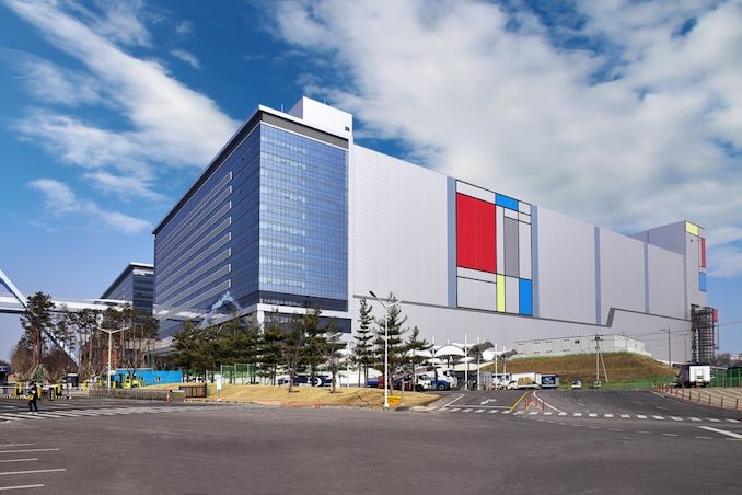
Samsung Foundry has started mass production of chips using its 6LPP and 7LPP manufacturing processes at its new V1 fab. The new facility employs one of the industry’s first production lines built from the ground up for technologies that heavily use EUV tools.
EUVL is a key enabler for Samsung’s next-generation leading-edge fabrication processes as it allows to reduce usage of multipatterning, and increases yields of chips architected for smaller technologies. Samsung currently uses EUVL equipment for its 6LPP and 7LPP nodes, and will expand its usage in future nodes such as 5LPE, 4LPE, 3GAE, and 3GAP processes.
| Advertised PPA Improvements of New Process Technologies Data announced by companies during conference calls, press briefings and in press releases |
||||||
| 7LPP vs 10LPE |
6LPP vs 7LPP |
5LPE vs 7LPP |
3GAE vs 7LPP |
|||
| Power | 50% | lower | 20% | 50% | ||
| Performance | 20% | ? | 10% | 35% | ||
| Area Reduction | 40% | ~9% | <20% | 40% | ||
Samsung Foundry’s 7LPP and 6LPP process technologies are used to make advanced mobile SoCs that will be shipped in Q1. The contract manufacturer of semiconductors does not disclose names of its client(s), but it is noteworthy that its 6LPP technology is not a part of its MPW (multi project wafer) shuttle program, which may indicate that the process is only available for Samsung itself and/or select customers who do not use MPWs.

Samsung’s 6LPP is a evolution of its 7LPP node that offers slightly higher (~10%) transistor density and lower power, but is compatible with, and can reuse IP initially developed for 7LPP. Furthermore, 6LPP supports smart structures for designers eager to invest in all-new IP, as well as multi diffusion break feature. Meanwhile, 5LPE promises to bring further advantages when it comes to power, performance, when compared to 6LPP.
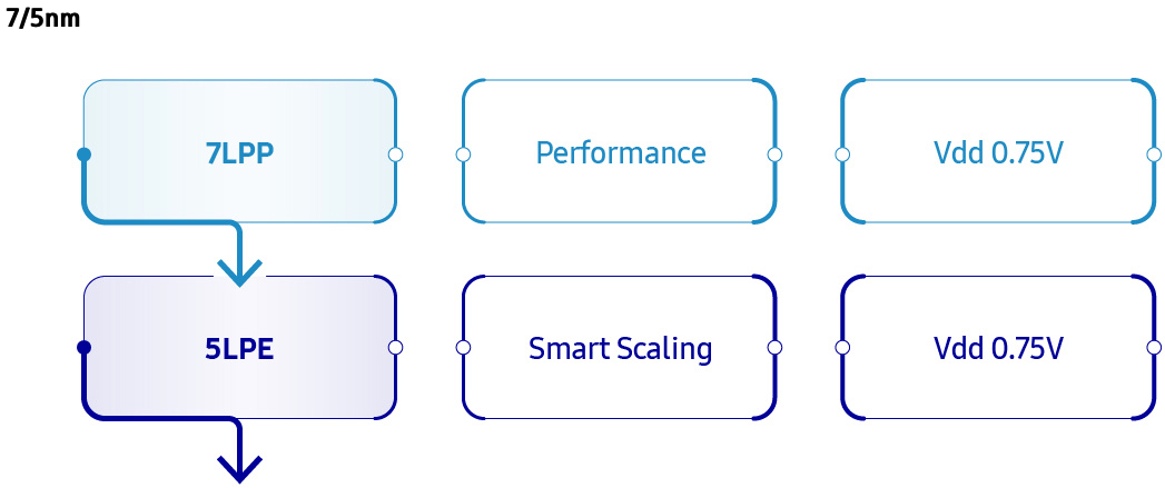
6LPP looks to be a limited offer node for select customers, whilst Samsung's focus in the future looks to be on its new 5LPE node.
| Global Manufacturing Sites of Samsung Foundry | ||||||||
| Name | 6-Line | S1 | S2 | S3 | S4 | V1 | ||
| Nodes | 180~65nm | 65~8nm | 65~11nm | 10nm~ | 65nm~ | 7nm~ | ||
| Location | Giheung, South Korea | Austin, Texas | Hwaseong, South Korea | |||||
| Wafer Size | 200 mm | 300 mm | ||||||
Samsung’s V1 fab is located in Hwaseong, Korea, adjacent to its S3 line, where Samsung started initial ramp of chips made using its 7LPP technology. The company began construction of V1 in February 2018, and initiated test wafer production in the second half of 2019. Samsung continues to ramp up its V1 fab now and says that by the end of the year its total capacity for EUV-enabled 7LPP and below nodes will be three times higher than it was in 2019. Meanwhile, cumulative investments in the V1 line will hit $6 billion by the end of 2020.

Related Reading:
- ASML Ramps Up EUV Scanners Production: 35 in 2020, Up to 50 in 2021
- EUV Demand is Up: EUV Device Manufacturer ASML Beats Sales Estimates
- Samsung Starts Mass Production of Chips Using Its 7nm EUV Process Tech
- Samsung Foundry Updates: 8LPU Added, EUVL on Track for HVM in 2019
- Samsung Completes Development of 5nm EUV Process Technology
Source: Samsung


29 Comments
View All Comments
levizx - Monday, February 24, 2020 - link
You are comparing 16FF+, TSMC's 2nd gen FinFET, to Samsung's 1st gen (14LPE) which had no competitor after TSMC scrapped their 1st gen (16FF).16FF+ should be compared to 14LPP, which Apple did NOT use.
Curiousland - Thursday, February 20, 2020 - link
Where is the proven technology and prototypes of 4nm and 3nm? Check before using title like that.rpg1966 - Thursday, February 20, 2020 - link
You don't need proven prototypes, to have built the fab with the expectation that it'll produce those designs.Fataliity - Thursday, February 20, 2020 - link
I could be wrong, but I'm pretty sure they have a prototype. Also, the pdk v0.1 is also available to begin designing on it. So they have finalized the requirements of what is legal in the designs.smilingcrow - Thursday, February 20, 2020 - link
5LPE v 7LPPArea Reduction <20%
Is that a mistake as not very impressive.
JKflipflop98 - Thursday, February 20, 2020 - link
Considering their "7nm" process is more like ~16nm or so. . .s.yu - Friday, February 21, 2020 - link
Samsung counts 7LPP-3LPE as a full node, which also shows in the numbers...just more marketing BS.s.yu - Friday, February 21, 2020 - link
GAE...edit, Anandtech, edit.mercucu1111 - Friday, February 21, 2020 - link
7LPP : 100MTr/mm^25LPE : 130MTr/mm^2
4LPE : 140MTr/mm^2
https://news.samsung.com/kr/카드-뉴스-5나노의-벽을-넘은-삼성전자-...
And They said that Area reduction is 25%. Not lesser than 20%.
Samsung's 5/4nm are half nodes. It is 5.5nm node in TSMC.
FullmetalTitan - Thursday, February 20, 2020 - link
Table at the bottom has an error:S1 line is shown as 200mm, but it should be 200mm. Only 6 line is 200mm
The global map below is correct, but does not match table