AMD Clarifies Comments on 7nm / 7nm+ for Future Products: EUV Not Specified
by Dr. Ian Cutress on March 5, 2020 6:50 PM EST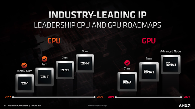
As part of AMD’s Financial Analyst Day 2020, the company gave the latest updates for its CPU and GPU roadmap. A lot of this we have seen before, with the company talking out to Zen 4 and Genoa on its datacenter CPU product line, out to Zen 3 and Ryzen 4000 with the consumer product line, and now with the RDNA/CDNA split between consumer and compute graphics. In previous graphs of a similar nature, AMD used the term ‘7nm+’ when referring to products beyond the first iteration of 7nm. AMD has today clarified to us that this does not mean they are using TSMC’s N7+ process node for those items.
TSMC has three high-level versions of its 7nm process:
- N7, which is the basic initial version using ‘DUV’ only tools (so no EUV),
- N7P, which is the second generation version of N7 which is also only DUV
- N7+, which is an EUV version of N7 for a number of layers in the metal stack
This nomenclature has been finalized within the past year or so.
Before this, AMD had presented various CPU and GPU roadmaps to the public. For the Zen 2 hardware, such as Ryzen 3000 series (Matisse), AMD had labeled this as ‘7nm’, which was all widely interpreted to mean TSMC’s N7 process. For future products, such as Zen 3, AMD had the slide listed as ‘7nm+’, which everyone had understood was ‘a better version of 7nm’.

Example Roadmap from CES 2018
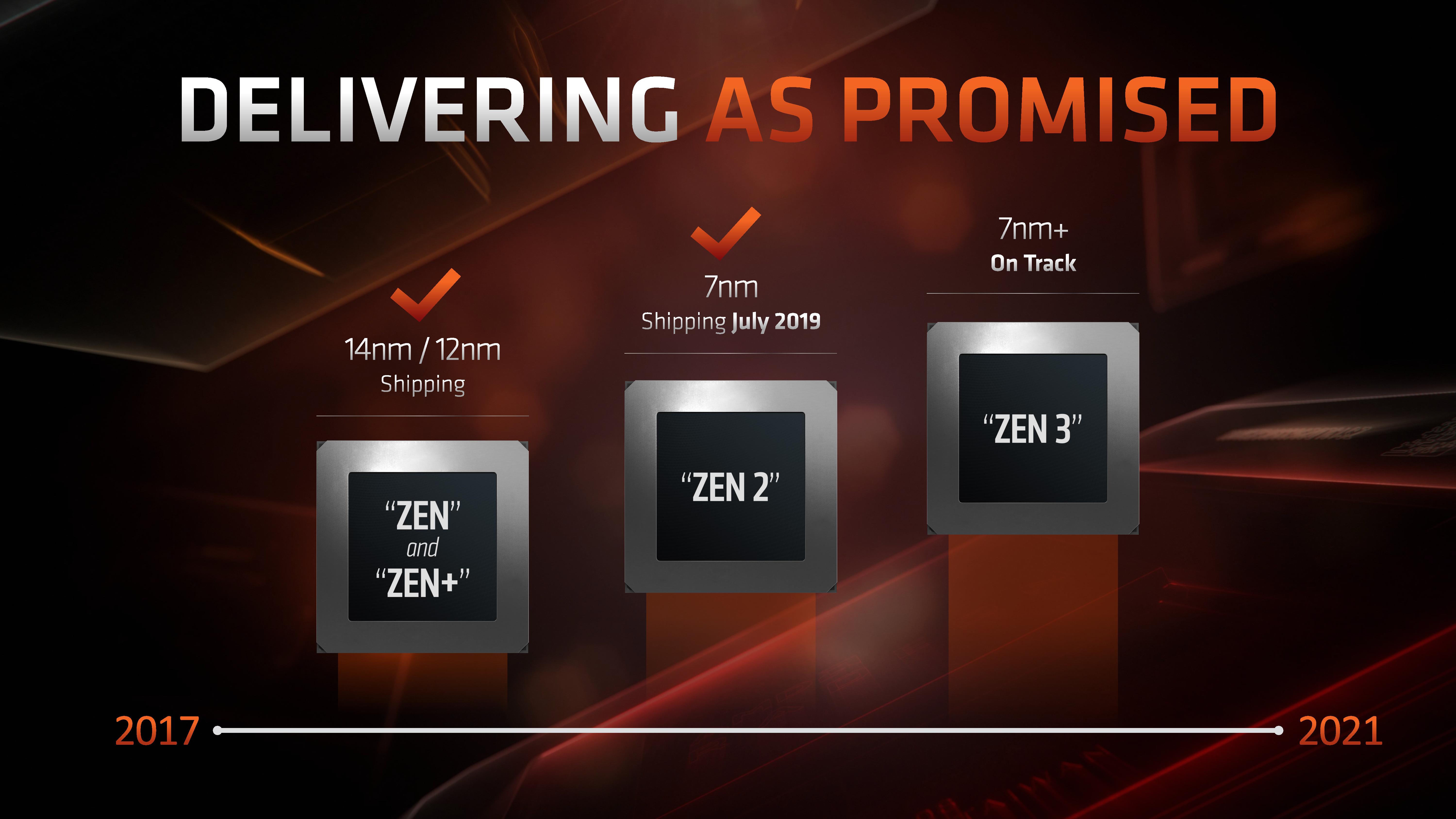
From Next Horizons in July 2019
Because AMD labeled those as 7nm+, when TSMC called its version of 7nm with EUV to be N7+, one of the obvious assumptions that people have made is that where AMD wrote 7nm+, it was to be on the N7+ process. We have since learned that this is not entirely correct.
In order to avoid confusion, AMD is dropping the ‘+’ from its roadmaps. In speaking with AMD, the company confirmed that its next generations of 7nm products are likely to use process enhancements and the best high-performance libraries for the target market, however it is not explicity stating whether this would be N7P or N7+, just that it will be ‘better’ than the base N7 used in its first 7nm line.
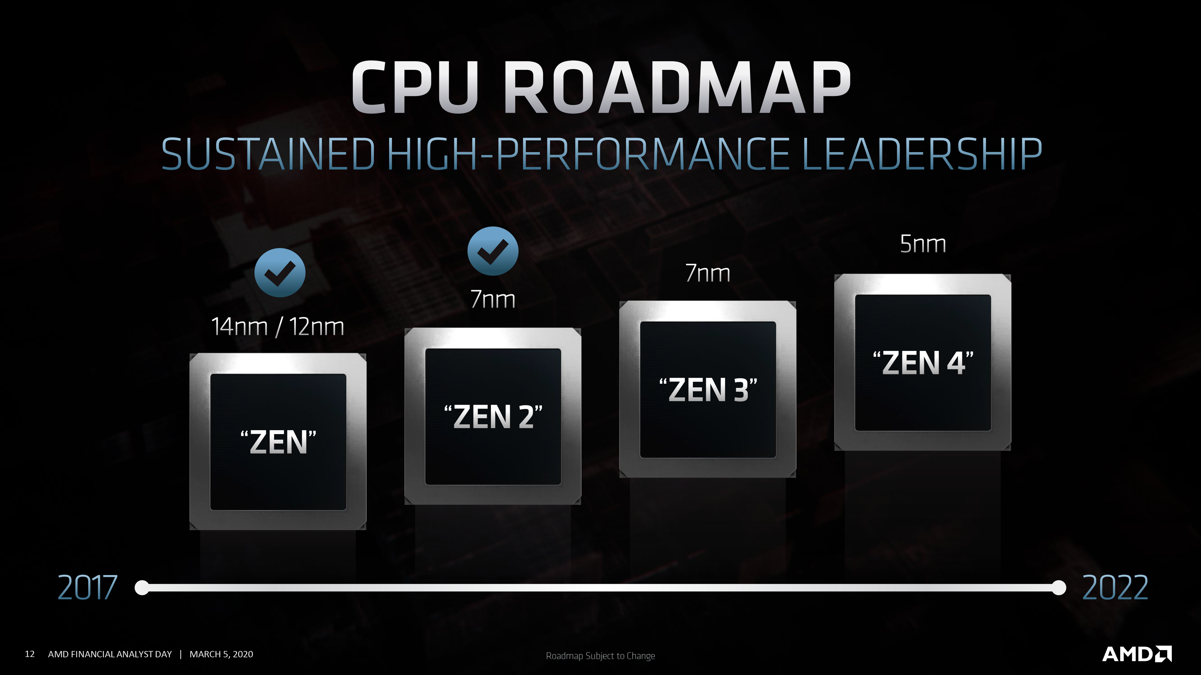
This doesn’t necessarily mean that AMD isn’t going to be using EUV in the future – we were told it will be on a case by case basis, and at this time they wanted to clarify that AMD is not making any specific clarifications of which version of 7nm from TSMC it plans to use. More will be detailed at future events.
Interested in more of our AMD Financial Analyst Day 2020 Coverage? Click here.


37 Comments
View All Comments
WaltC - Friday, March 6, 2020 - link
Again, Papermaster was very clear on the fact that + improvement had been rolled into their 7nm standard production node, I thought--what I get from that is while 7nm is called +, it now includes many of the most important + features. Either Papermaster misspoke or else this 7nm is a better node than the first one--which would not be surprising at all.CiccioB - Friday, March 6, 2020 - link
I think AMD just hoped for 7n+ (EUV) to be ready for RDNA2 and Zen3 but they were not that lucky as for plain 7nm that ramped up quite well for them.So they just made a turn back and are now targeting the other <7nm options hinting that 7nm+ meant whatever after plain 7nm that is good enough
Fataliity - Friday, March 6, 2020 - link
It's still on the same process. TSMC just renamed "7nm+" to "N7". There are multiple variants of N7 under the same node name. For example7nm HPC
N7
N7P
N7+
That doesn't mean that it's no longer 7nm+. It just means TSMC is no longer calling it "7nm+" So neither is AMD.
dotjaz - Friday, March 6, 2020 - link
That's a load of sh*t and you know it. TSMC NEVER EVER EVER called any process "7nm+". AMD calls the improved 7nm "7nm+" just like when they called 12LP "14nm+". It has NOTHING to do with TSMC's naming scheme.CiccioB - Saturday, March 7, 2020 - link
This is not true at all.TSMC has ALWAYS make distinction between its N7 versions:
N7 for the DUV plain version, 7N+ for the EUV version and only lately N7P for the improved 7N on DUV.
The rest of the world, that does not use TSMC PP names to make people understand the kind of PP used has always used the terms 7nm for the plain version and 7nm+ for the EUV version.
Look in the Internet about any article written with the word '7nm+' in it and see what they are referring to.
This was going on since TSMC has announced they were using EUV for a version of their 7nm PP.
Now, this identifiers used for the slide last year were clear: 7nm for plain, 7nm+ for the EUV version.
7NP just came out lately, 6 months ago. Before it it didn't exists at all.
What happened is simply that AMD targeted 7mn+ (that is TSMC N7+) for the next generation of their product but now that PP is not mature as they thought it would be, and in fact, TSMC has now created a 7NP version to improve plain 7nm (N7) a little bit without having to wait for 7nm+ (N7+) to be ready, which would improve over N7 much more than N7P.
In the original slide that is dated 2017, a couple of years before 7NP was born, there was also a refer to 14nm+, that surely didn't meant 'anything after 14nm PP' as AMD want now us to intend its 7nm+.
This change in AMD nomenclature is simply a way to mask the fact that they missed the 7NM+ rendezvous (not their fault, but still a miss in their written roadmap) and have to fall back to a less performer PP that is the patched N7 (N7P).
LedHed - Friday, March 6, 2020 - link
Can you confirm that Zen 2 chips, like the 3950X, were made using the base N7 processing?You almost said this, but you never actually did. Is this the case?
dotjaz - Friday, March 6, 2020 - link
Nope, they are using a modified version with very different scaling/density. N7 Large Die appeared on TSMC's PPT once and "Large Die" certainly don't mean it's actually large. Zen2 chiplets are smaller than many baseline N7/N7P/N7+ dies such as A13, S865, K990 etcFataliity - Friday, March 6, 2020 - link
At the end of their financial analyst day, AMD reiterated when asked a question about this that yes, it's still on the same process, but TSMC no longer calls 7nm+ "7nm+", its all encompassed under the "N7" name. So they changed their nomenclature to match TSMC's nomenclature.dotjaz - Friday, March 6, 2020 - link
TSMC never called anything "7nm+" they can't change from what they never used.dotjaz - Friday, March 6, 2020 - link
"Our second generation 7nm (N7+) technology entered risk production in August 2018" straight from TSMC website. They didn't call it 7nm+ while referring to N7+ explicitly.