The Intel Lakefield Deep Dive: Everything To Know About the First x86 Hybrid CPU
by Dr. Ian Cutress on July 2, 2020 9:00 AM ESTThermal Management on Stacked Silicon
With a standard processor design, there is a single piece of silicon doing all the work and generating the heat – it’s bonded to the package (which doesn’t do any work) and then depending on the implementation, there’s some adhesive to either a cooler or a headspreader then a cooler. When moving to a stacked chiplet design, it gets a bit more complicated.
Having two bits of silicon that ‘do work’, even if one is the heavy compute die and the other is an active interposer taking care of USB and audio and things, does mean that there’s a thermal gradient between the silicon, and depending on the bonding, potential for thermal hotspots and build-up. Lakefield makes it even more complex, by having an additional DRAM package placed on top but not directly bonded.
We can take each of these issues independently. For the case of die-on-die interaction, there is a lot of research going into this area. Discussions and development about fluidic channels between two hot silicon dies have been going on for a decade or longer in academia, and Intel has mentioned it a number of times, especially when relating to a potential solution of its new die-to-die stacking technology.
They key here is hot dies, with thermal hotspots. As with a standard silicon design, ideally it is best to keep two high-powered areas separate, as it gives a number of benefits with power delivery, cooling, and signal integrity. With a stacked die, it is best to not have hotspots directly on top of each other, for similar reasons. Despite Intel using its leading edge 10+ process node for the compute die, the base die is using 22FFL, which is Intel’s low power implementation of its 14nm process. Not only that, but the base die is only dealing with IO, such as USB and PCIe 3.0, which is essentially fixed bandwidth and energy costs. What we have here is a high-powered die on top of a low powered die, and as such thermal issues between the two silicon die, especially in a low TDP device like Lakefield (7W TDP), are not an issue.
What is an issue is how the compute die gets rid of the heat. On the bottom it can do convection by being bonded to more silicon, but the top is ultimately blocked by that DRAM die. As you can see in the image above, there’s a big air gap between the two.
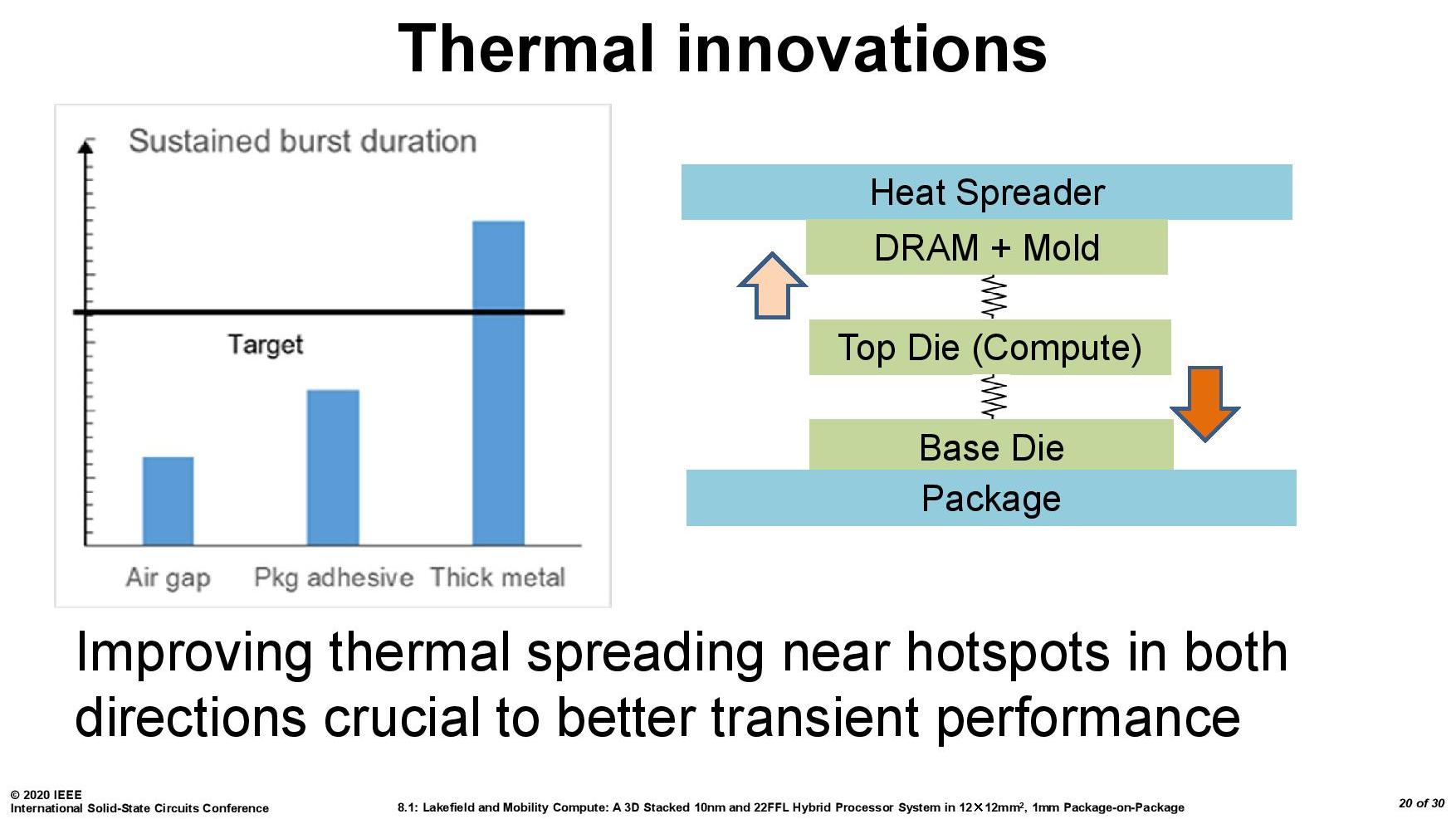
As part of the Lakefield design, Intel had to add in a number of design changes in order to make the thermals work. A lot of work can be done with the silicon design itself, such as matching up hotspots in the right area, using suitable thickness of metals in various layers, and rearranging the floorplan to reduce localized power density. Ultimately both increasing the thermal mass and the potential dissipation becomes high priorities.
Lakefield CPUs have a sustained power limit of 7 watts – this is defined in the specifications. Intel also has another limit, known as the turbo power limit. At Intel’s Architecture Day, the company stated that the turbo power limit was 27 watts, however in the recent product briefing, we were told is set at 9.5 W. Historically Intel will let its OEM partners (Samsung, Lenovo, Microsoft) choose its own values for these based on how well the design implements its cooling – passive vs active and heatsink mass and things like this. Intel also has another factor of turbo time, essentially a measure of how long the turbo power can be sustained for.
When we initially asked Intel for this value, they refused to tell us, stating that it is proprietary information. After I asked again after a group call on the product, I got the same answer, despite the fact that I informed the Lakefield team that Intel has historically given this information out. Later on, I found out through my European peers that in a separate briefing, they gave the value of 28 seconds, to which Intel emailed me this several hours afterwards. This value can also be set by OEMs.
Then I subsequently found one of Intel’s ISSCC slides.
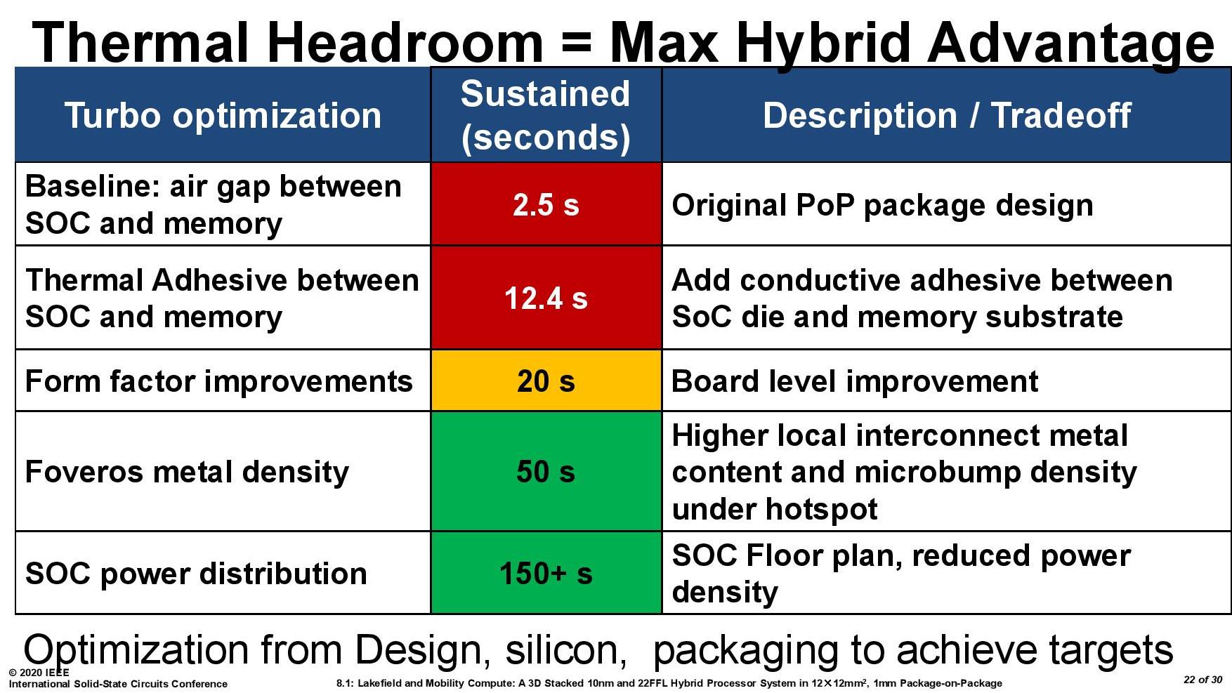
This slide shows that a basic implementation would only allow sustained power for 2.5 seconds. Adding in an adhesive between the top die and the DRAM moves up to 12.4 seconds, and then improving the system cooling goes up to 20 seconds. The rest of the improvements work below the compute die: a sizeable improvement comes from increasing the die-to-die metal density, and then an optimized power floor plan which in total gives sustained power support for 150+ seconds.


221 Comments
View All Comments
ichaya - Sunday, July 12, 2020 - link
You've claimed ARM64 has a code density advantage without any evidence for a few posts now. Being byte-aligned has advantages too, which are clear in the paper with the real world program! You're welcome to provide more real world evidence!We're changing the goal posts now with new numbers, you can't estimate IPC based on one specific INTrate2006 test, and assume it's similar across other workloads as well. If we just stick to INTrate2006, IPC seems within 5% where Graviton 2 has twice the cache of AMD Epyc 7742.
Comparing a top-line power number like you were doing is irrelevant when features like AVX can easily blow past any power envelope you might have, and one chip lacks the feature.
Wilco1 - Sunday, July 12, 2020 - link
No, I am stating that AArch64 has better code density as a fact. Maybe 5 years ago you could argue about it as AArch64 was still relatively new, but today that's not even disputable. So check it out if you'd like to see it for yourself.I used the overall intrate result to get an accurate IPC comparison. If you do the math correctly you'll see that Graviton 2 has 12% higher IPC than EPYC 7742.
At the end of the day what matters is performance, perf/W and cost. Whether you have AVX or not is not relevant in this comparison - EPYC 7742 uses the same amount of power whether it executes AVX code or not.
ichaya - Tuesday, July 14, 2020 - link
This is not the first time I've seen someone look at single thread performance and disregard everything else. All Graviton 2 and A13 single thread gains can be attributed to large (100~200% more) shared L2/L3 caches, and when compared with x86, 5% or even 75% IPC gains turn out to be ~10% less real world performance or ~10% more with marginal power use difference on 7nm. AMD has everything from a 15W to 280W chip.For multi-threaded, the Graviton 2 looks better, but the 64 vcpu EPYC 2 c5a.16xlarge (144MB L2+L3) AWS instance costs the same as the 64 core Graviton 2 m6g.16xlarge (96MB L2+L3) instance and delvers equivalent performance on real world tasks while having 1/2 the real cores, 1/2 the system RAM and 50% more L2+L3.
perf/W/$ is important, and since ARM has always been on the lower end of W and $, it can be hard to see past it. If you can compare cache sizes, power and real world performance, the only thing revolutionary is the fact that Amazon, Apple and the ARM ecosystem have come this far in a few years. The overall features (AVX2+SMT among others) and openness still leaves a lot to be desired.
Wilco1 - Wednesday, July 15, 2020 - link
Single threaded performance is important in showing that x86 does no longer have the big advantage it once used to have. Overall throughput is well correlated with single thread performance, you can see that clearly in the results we discussed. Do you believe 64 Graviton 1 cores would do equally well against 7742 if they had the same huge caches?I haven't seen serious benchmarks on c5a, do you have a link? With 32 cores at 3.3GHz it should burn well over 200W, not an improvement...
It's not that revolutionary if you followed the rapid increase of single thread performance over the last 5 years. Smartphones paid for the progress in microarchitecture and process technology that enabled competitive Arm servers (it helped AMD surpass Intel as well). I don't believe SMT or AVX are useful - 128 cores in Altra Max will beat 64 cores with SMT+AVX on performance and area at similar power.
As for AVX, this article discusses how Intel's latest CPU disables AVX... Linus had some interesting comments recently about the fragmentation of the many AVX variants. Then there are all the unresolved clocking and power issues. It's a mess.
ichaya - Thursday, July 16, 2020 - link
If there was a significant power difference between m6g.16xlarge and c5a.16xlarge, they would be priced differently. 128GB of RAM can't be more than ~15W.Single thread performance can help multi-thread performance up to a point, but SMT, non-boost clocks, and biasing towards TLP more than ILP (like an in-order GPU) can hurt single thread performance at the expense of more multi-threaded throughput.
AVX-512 is a mess, but AVX2 is worth having in most contexts now. Maybe some AVX512 instructions worth having will make it into a AVX2.1 which can completely supersede AVX2. For the price of Lakefield, there are certainly more attractive options, though compatibility, packaging and performance can trump battery life.
Wilco1 - Thursday, July 16, 2020 - link
Well there is a much better comparison, c6g.16xlarge has 128GB and is 12% cheaper than c5a.16xlarge. More than enough to pay for the electricity cost of the 280W TDP of c5a.Yes you can optimize for multithreaded throughput but SMT remains questionable, especially for large core counts. Why add SMT when you could just add some more cores?
Indeed AVX512 is worse, and could be removed without anyone missing it. Lakefield battery life comparisons are in, the Atom curse has struck yet again...
ichaya - Thursday, July 16, 2020 - link
12% is probably more the amount of subsidies these instances are getting. Amazon has a very very long history of putting any profit margins back into growth. Either that, or 128GB of RAM is 100W+!SMT is perhaps the lowest level at which TLP can be extracted, recent multi-core Atoms don't have it, but for server/workstation tasks like compilation, DB engine or even general multi-tasking, it's well worth it.
Wilco1 - Friday, July 17, 2020 - link
Graviton 2 is less than a third of the silicon area of EPYC so cheaper to make. 128GB server DRAM costs over $1000, which is why the 256GB/512GB versions are more expensive. The power cost of extra DRAM is a tiny fraction of that.There are tasks where SMT helps but equally there also tasks where it is slower. So it looks great on marketing slides where you just show the best cases, but overall it is a small gain.
ichaya - Saturday, July 18, 2020 - link
I wouldn't call a 64 vcpu (180W) system beating or equaling a 64 core (110W) system in web serving/DB and code compilation a small gain. The tasks where SMT hurts is basically single threaded JS, which is just such a shame. Shame! I don't think POWER, SPARC and others have been wrong in having added SMT years ago.For code compilation and DB the differences are 50%-100%+ making perf/W/$ very competitive.
https://www.phoronix.com/scan.php?page=article&...
This article also seems to mention SMT might make an appearance in the next Neoverse N* chips: https://www.nextplatform.com/2019/02/28/arm-sharpe...
Wilco1 - Sunday, July 19, 2020 - link
The Phoronix link has various benchmarks that aren't even running identical code between different ISAs (eg. Linux kernel compile). So it's not anywhere near a fair CPU comparison like SPEC. And this: https://openbenchmarking.org/result/1907314-AS-RYZ... shows SMT gives almost no gain on multithreaded benchmarks once you stop cherry picking the good results and ignore the bad ones...Even if we just consider the benchmarks with the largest SMT speedup, Coremark and 7-zip have good SMT gains of 41% and 32%, but m6g *still* outperforms c5a by 5% and 24%.
So the best SMT gain combined with a 32% frequency advantage and 4 times the L3 cache is still not enough to provide equal per-thread performance!