The Intel Lakefield Deep Dive: Everything To Know About the First x86 Hybrid CPU
by Dr. Ian Cutress on July 2, 2020 9:00 AM ESTThermal Management on Stacked Silicon
With a standard processor design, there is a single piece of silicon doing all the work and generating the heat – it’s bonded to the package (which doesn’t do any work) and then depending on the implementation, there’s some adhesive to either a cooler or a headspreader then a cooler. When moving to a stacked chiplet design, it gets a bit more complicated.
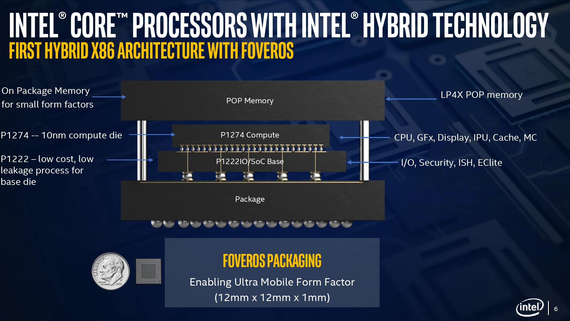
Having two bits of silicon that ‘do work’, even if one is the heavy compute die and the other is an active interposer taking care of USB and audio and things, does mean that there’s a thermal gradient between the silicon, and depending on the bonding, potential for thermal hotspots and build-up. Lakefield makes it even more complex, by having an additional DRAM package placed on top but not directly bonded.
We can take each of these issues independently. For the case of die-on-die interaction, there is a lot of research going into this area. Discussions and development about fluidic channels between two hot silicon dies have been going on for a decade or longer in academia, and Intel has mentioned it a number of times, especially when relating to a potential solution of its new die-to-die stacking technology.
They key here is hot dies, with thermal hotspots. As with a standard silicon design, ideally it is best to keep two high-powered areas separate, as it gives a number of benefits with power delivery, cooling, and signal integrity. With a stacked die, it is best to not have hotspots directly on top of each other, for similar reasons. Despite Intel using its leading edge 10+ process node for the compute die, the base die is using 22FFL, which is Intel’s low power implementation of its 14nm process. Not only that, but the base die is only dealing with IO, such as USB and PCIe 3.0, which is essentially fixed bandwidth and energy costs. What we have here is a high-powered die on top of a low powered die, and as such thermal issues between the two silicon die, especially in a low TDP device like Lakefield (7W TDP), are not an issue.
What is an issue is how the compute die gets rid of the heat. On the bottom it can do convection by being bonded to more silicon, but the top is ultimately blocked by that DRAM die. As you can see in the image above, there’s a big air gap between the two.
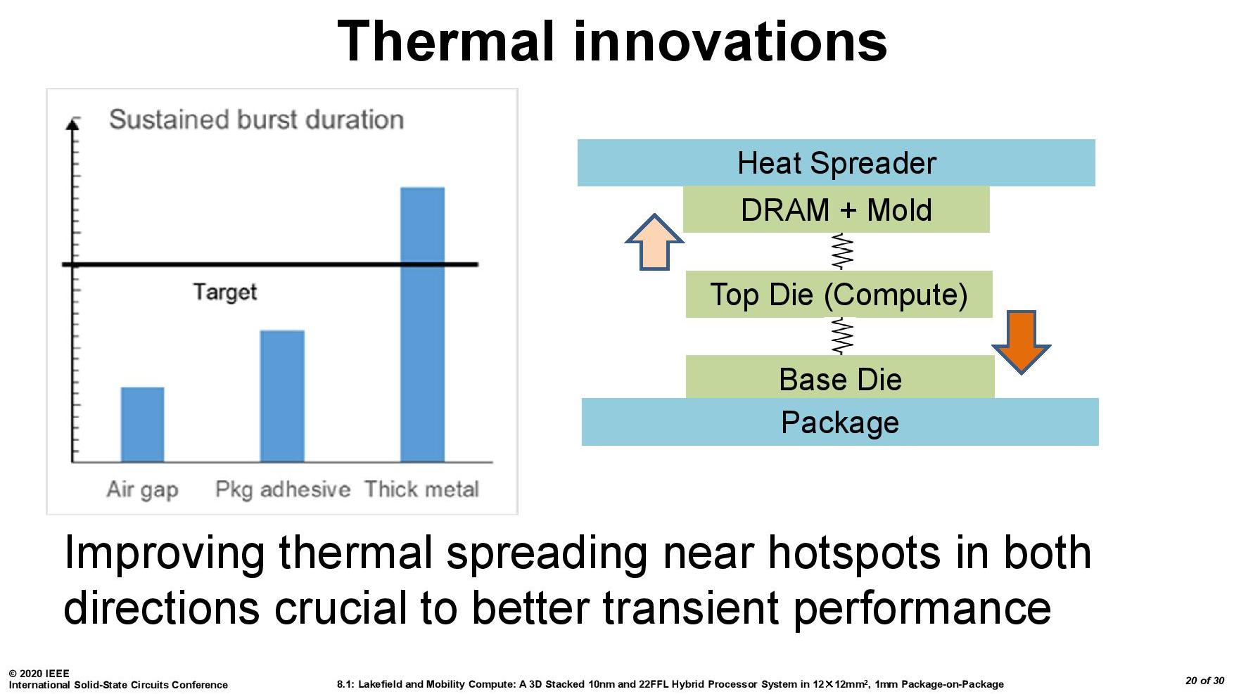
As part of the Lakefield design, Intel had to add in a number of design changes in order to make the thermals work. A lot of work can be done with the silicon design itself, such as matching up hotspots in the right area, using suitable thickness of metals in various layers, and rearranging the floorplan to reduce localized power density. Ultimately both increasing the thermal mass and the potential dissipation becomes high priorities.
Lakefield CPUs have a sustained power limit of 7 watts – this is defined in the specifications. Intel also has another limit, known as the turbo power limit. At Intel’s Architecture Day, the company stated that the turbo power limit was 27 watts, however in the recent product briefing, we were told is set at 9.5 W. Historically Intel will let its OEM partners (Samsung, Lenovo, Microsoft) choose its own values for these based on how well the design implements its cooling – passive vs active and heatsink mass and things like this. Intel also has another factor of turbo time, essentially a measure of how long the turbo power can be sustained for.
When we initially asked Intel for this value, they refused to tell us, stating that it is proprietary information. After I asked again after a group call on the product, I got the same answer, despite the fact that I informed the Lakefield team that Intel has historically given this information out. Later on, I found out through my European peers that in a separate briefing, they gave the value of 28 seconds, to which Intel emailed me this several hours afterwards. This value can also be set by OEMs.
Then I subsequently found one of Intel’s ISSCC slides.
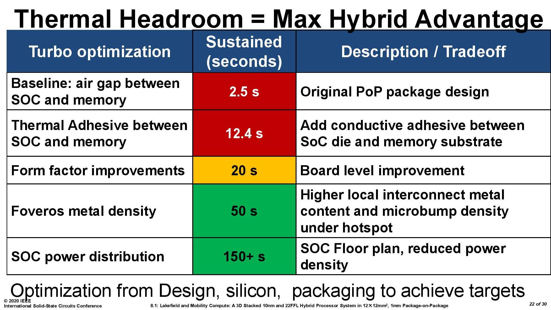
This slide shows that a basic implementation would only allow sustained power for 2.5 seconds. Adding in an adhesive between the top die and the DRAM moves up to 12.4 seconds, and then improving the system cooling goes up to 20 seconds. The rest of the improvements work below the compute die: a sizeable improvement comes from increasing the die-to-die metal density, and then an optimized power floor plan which in total gives sustained power support for 150+ seconds.


221 Comments
View All Comments
returnzer0 - Friday, July 3, 2020 - link
So no, they did not, in fact, read the same article.s.yu - Monday, July 6, 2020 - link
Mystery solved!vanilla_gorilla - Friday, July 3, 2020 - link
https://www.anandtech.com/show/15877/intel-hybrid-..."At the top is the single Sunny Cove core, also present in Ice Lake. Intel has stated that it has physically removed the AVX-512 part of the silicon, however we can still see it in the die shot. This is despite the fact that it can’t be used in this design due to one of the main limitations of a hybrid CPU. We’ll cover that more in a later topic."
It was NOT physically removed but it cannot be used so it doesn't really matter. In practice this will have no AVX-512.
dotjaz - Friday, July 3, 2020 - link
Also "However, all modern software assumes a homogeneous processor", that's why they have to support exactly the same ISA extensions. I didn't realise Windows is the only modern software in existence.Meteor2 - Friday, July 3, 2020 - link
Why so rude, dotjaz?dotjaz - Saturday, July 4, 2020 - link
So which part is rude? Is this rude asking you what's rude? Sorry your feelings got hurt. There, happy now?jospoortvliet - Sunday, July 5, 2020 - link
Linux also expects it. Modern enough?jeremyshaw - Thursday, July 2, 2020 - link
Good. This action ensures this segment of products will be easier to emulate on arm, helping to tear these products away from Intel's grasp.Kangal - Sunday, July 5, 2020 - link
To be honest, this is a great innovation.It's just the execution is quite lacking, and on top of that, it's a couple years too late.
Just imagine a SoC such as:
3x Big processor (Intel Core M), eg/ Core i7-8500Y
5x Small processor (Intel Atom), eg/ Atom x7-Z8750
Dynamic Scaling:
(Idle) 4x Small Cores run at 500MHz at Idle
(Very-low power) 4x Small Cores clock starting at 1.0GHz
(Low-power use) 5x Small Cores clock upto 2.5GHz
(Medium power) 3x Big Cores starting at 1.5GHz, 5x Small Cores upto 2.5GHz
(Regular power) 3x Big Cores at 2.0GHz, 5x Small Cores at 2.0GHz
(High-power use) 3x Big Cores at 3.0GHz, 5x Small Cores at 2.0GHz
(Very-high power) 3x Big Cores at 4.0GHz, 5x Small Cores at 2.5GHz
(Max-power use) 1x Big Cores at 5.0GHz, 2x Big Cores at 4.0GHz, 5x Small Cores at 2.5GHz
Kangal - Sunday, July 5, 2020 - link
Now imagine all of this, competing against AMD.Their 12nm node is fairly competitive against Intel's 14nm. And their Zen+ architecture is somewhat competitive against Intel's Skylake architecture. So comparing the above Hybrid Processor, to a 4c/8t (eg/ Ryzen-3780U). Well that's a no contest victory for Intel. And AMD would struggle to fit those technologies into a 8-core laptop processor, so there would be no threat from above.
Once AMD steps up to either Zen2 architecture, or 7nm node, or both!...
....that's when things get heated. Since in the 15W / Ultrabook market, the above setup by Intel would secure a slim victory against similar 4c/8t AMD processor. But when you step up to the 25W / Laptop market, then AMD will pull ahead with their 8c/16t processor. However at least in this scenario, Intel has a good showing of their competitiveness and capabilities. That works upto 2021, but after that, Intel will have to make noticeable performance improvements to both Big/Small Core architectures, AND, they will have to make substantial efficiency improvements on the lithography side (maybe execute on their 8nm nodes, versus TSMC's 5nm).
First question, why use examples of Cherry Trail and Amber Lake?
Well, they're both on Intel's (pretty good) 14nm node. Also this is the most efficient "Small Core" Atom architecture that Intel has. Later produced Intel Pentium/Celeron/Atom processors come from the same family, however, they're designed for higher energy consumption. Whereas the "Big Core" stated above is a Core M processor (now rebranded as a Core i7-Y), and it is the latest and best they have when it comes to performance whilst maintaining efficiency.
Why the 3/5 Split you may ask?
Well, the most useful is the first/main thread. Followed closely by the second thread as most code has evolved for Dual-Cores in the past 20 years. And somewhat important is the third core, as we've also had an evolution to Quad-Cores in the past 10 years. However, most code hasn't made the full transition from single to dual threads, the same way that dual threads haven't translated well to quad threads. So instead of 2+6 split, which will have some performance drops on Quad thread code, it's better to go for 3+5. So you may ask, then why not just go for an even 4+4 split? Well, most of those quad threads don't utilise the 4th core very well, so we can make do by relegating that to a Small Core instead. This saves us some efficiency, which is what we want to achieve with this concept in the first place. The least energy using split would be 0+8. The most performant split would be 8+0. So this 3+5 split is basically the best of both worlds, since you will get 90% of the single-threaded performance, 70% of the multi-threaded performance, and 50% of the energy expenditure characteristics. So it's not perfect, but it's the closest you can get there... until the code evolves further. And we've started transitioning codes running for 8-core processors only around 2015-2017, so there's a good chance we aren't going to see the evolution tipping point until around 2025.