The Intel Lakefield Deep Dive: Everything To Know About the First x86 Hybrid CPU
by Dr. Ian Cutress on July 2, 2020 9:00 AM ESTLakefield: Top Die to Bottom Die
At the top is the compute die, featuring the compute cores, the graphics, and the display engines for the monitors.

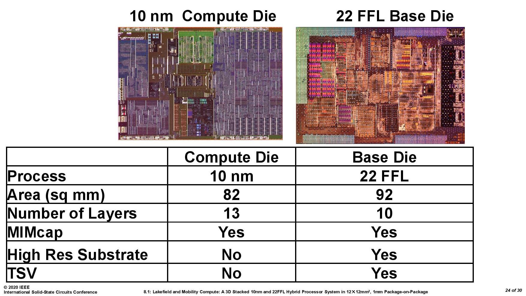
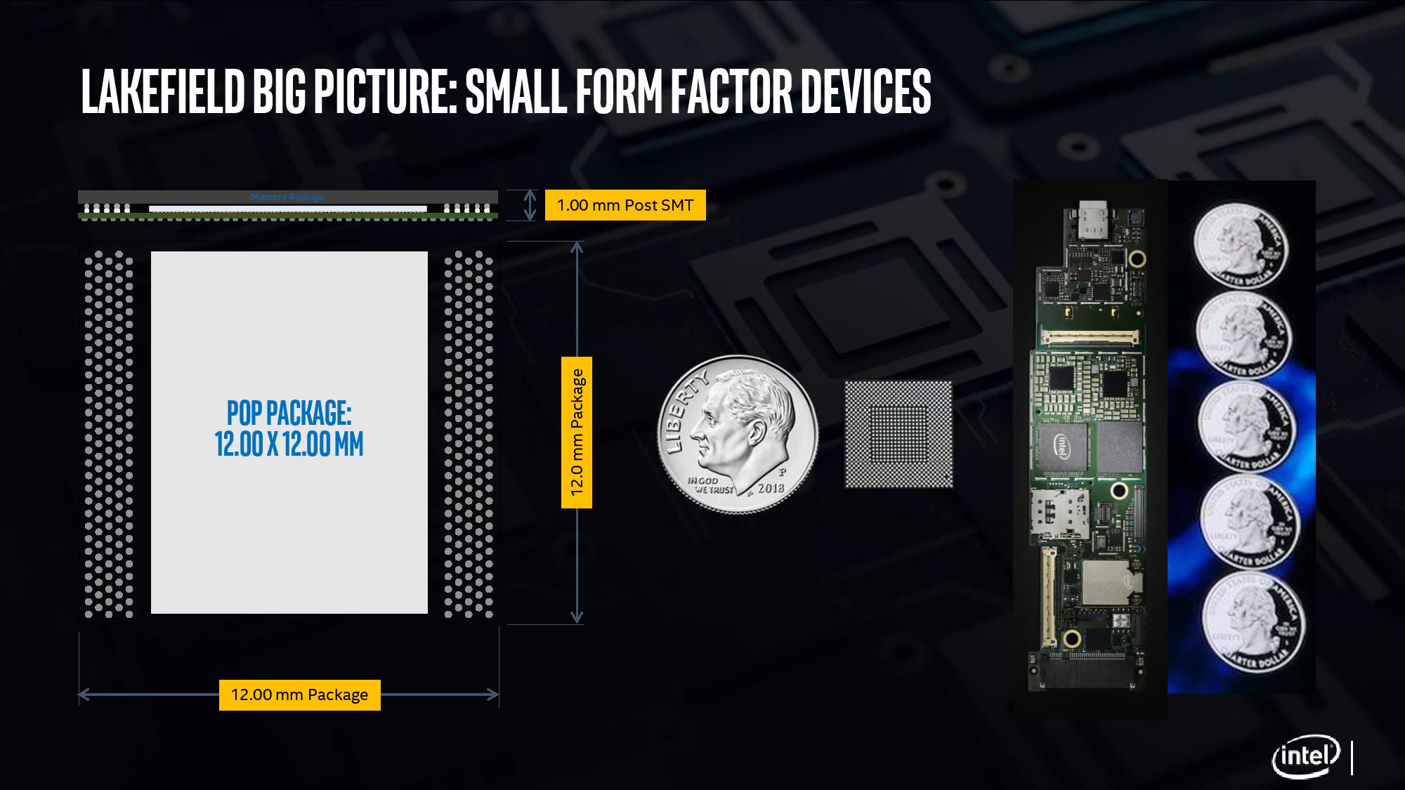
It might be easier to imagine it as the image above. The whole design fits into physical dimensions of 12 mm by 12 mm, or 0.47 inch by 0.47 inch, which means the internal silicon dies are actually smaller than this. Intel has previously published that the base peripheral interposer silicon is 92 mm2, and the top compute die is 82 mm2.
Compute Die
Where most of the magic happens is on the top compute die. This is the piece of silicon built on Intel’s most advanced 10+ nm process node and contains the big core, the small cores, the graphics, the display engines, the image processing unit, and all the point-to-point connectivity. The best image of this die looks something like this:
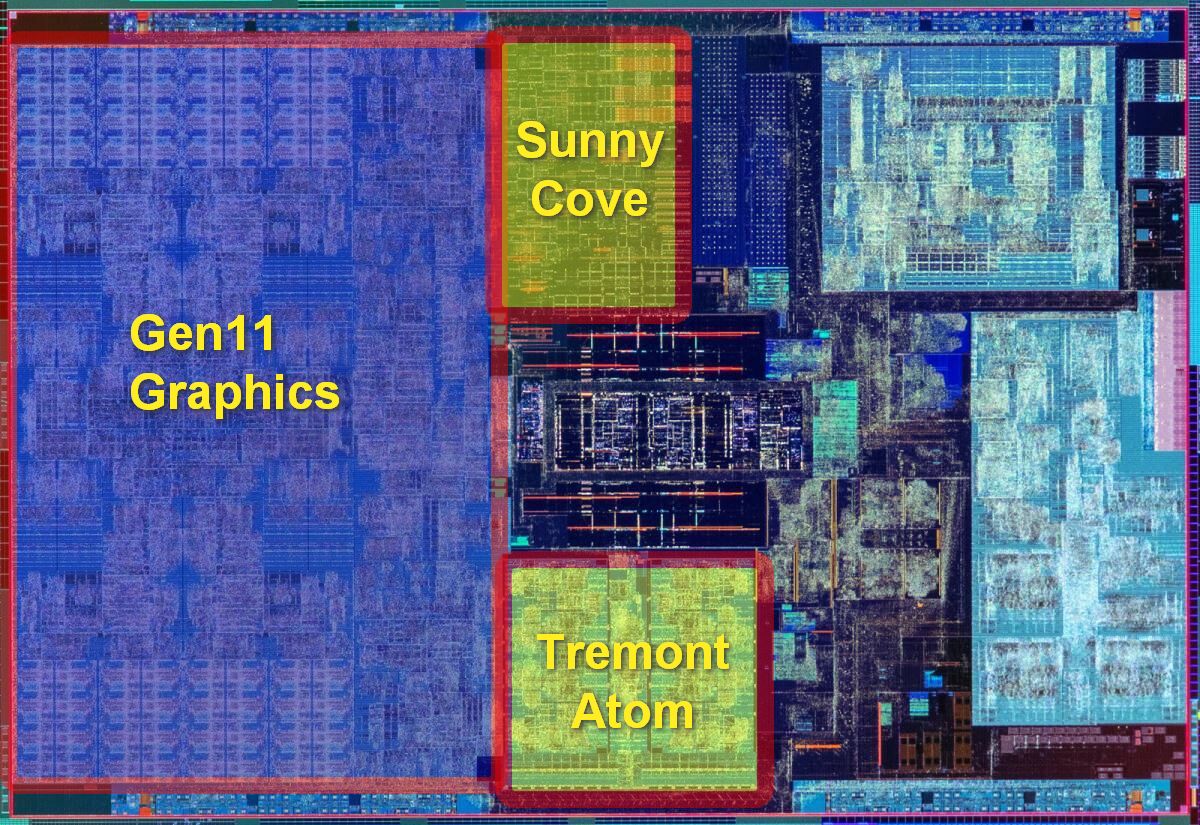
The big block on the left is the Gen 11 graphics, and is about 37% of the top compute die. This is the same graphics core configuration as what we’ve seen on Intel’s Ice Lake mobile CPUs, which is also built on the same 10+ process.
At the top is the single Sunny Cove core, also present in Ice Lake. Intel has stated that it has physically removed the AVX-512 part of the silicon, however we can still see it in the die shot. This is despite the fact that it can’t be used in this design due to one of the main limitations of a hybrid CPU. We’ll cover that more in a later topic.
At the bottom in the middle are the four Tremont Atom cores, which are set to do most of the heavy lifting (that isn’t latency sensitive) in this processor. It is worth noting the relative sizes of the single Sunny Cove core compared to the four Tremont Atom cores, whereby it seems we could fit around three Tremont cores in the same size as a Sunny Cove.
On this top compute die, the full contents are as follows:
- 1 x Sunny Cove core, with 512 KiB L2 cache
- 4 x Tremont Atom cores, with a combined 1536 KiB of L2 cache between them
- 4 MB of last level cache
- The uncore and ring interconnect
- 64 EUs of Gen11 Graphics
- Gen11 Display engines, 2 x DP 1.4, 2x DPHY 1.2,
- Gen11 Media Core, supporting 4K60 / 8K30
- Intel’s Image Processing Unit (IPU) v5.5, up to 6x 16MP cameras
- JTAG, Debug, SVID, P-Unit etc
- LPDDR4X-4267 Memory Controller
Compared to Ice Lake mobile silicon, which measures in at 122.52 mm2, this top compute die is officially given as 82.x mm2. It’s worth noting that the Ice Lake die also contains what Lakefield has on the base die as well. This top die has been quoted as having 4.05 billion transistors and 13 metal layers. For those playing a transistor density game at home, this top die averages 49.4 million transistors per square millimeter.
Base Die / Interposer Die
The base interposer die is, by contrast, a lot simpler. It is built on Intel’s 22FFL process, which despite the name is actually an optimized power version of Intel’s 14nm process with some relaxed rules to allow for ultra-efficient IO development. The benefit of 22FFL being a ‘relaxed’ variant of Intel’s own 14nm process also means it is simpler to make, and really chip by comparison to the 10+ design of the compute die. Intel could make these 22FFL silicon parts all year and not break a sweat. The only complex bit comes in the die-to-die connectivity.
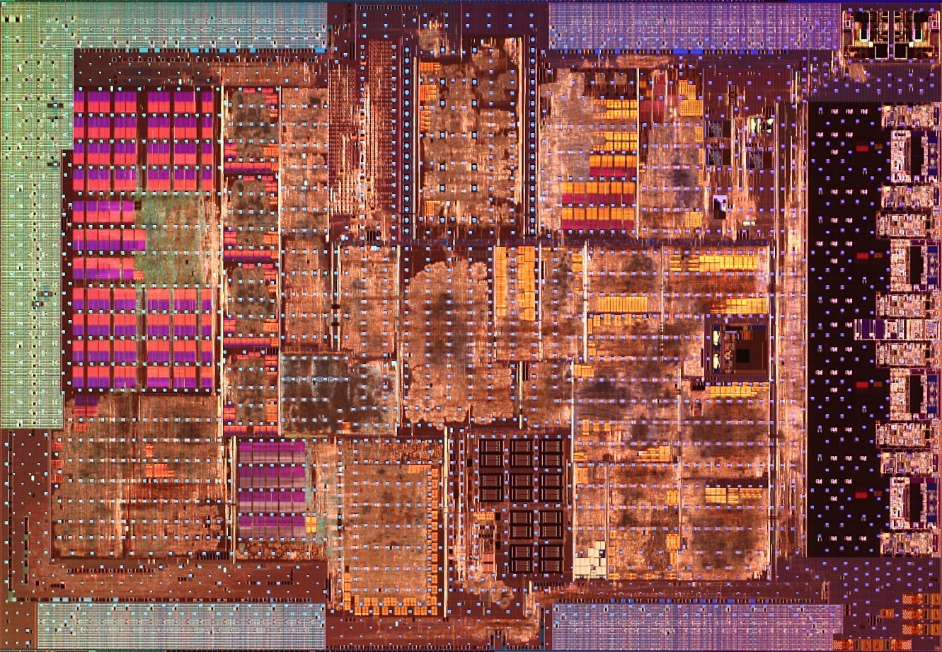
The small white dots on the diagram are meant to be the positions of the die-to-die bonding patches. Intel has quoted this base silicon die as having 10 metal layers, and measuring 92.x mm2 for only only 0.65 billion transistors. Again, for those playing at home, this equates to an average density of 7.07 million transistors per square millimeter.
On this bottom die, along with all the management for the die-to-die interconnects, we get the following connectivity which is all standards based:
- Audio Codec
- USB 2.0, USB 3.2 Gen x
- UFS 3.x
- PCIe Gen 3.0
- Sensor Hub for always-on support
- I3C, SDIO, CSE, SPI/I2C
One element key to the base interposer and IO silicon is that it also has to carry power up to the compute die. With the compute die being on top to aid in the cooling configuration, it still has to get power from somewhere. Because the compute die is the more power hungry part of the design, it needs dedicated power connectivity through the package. Whereas all the data signals can move around from the compute die to the peripheral die, the power needs to go straight through. As a result, there are a number of power oriented ‘through silicon vias’ (TSVs) that have to be built into the design of the peripheral part of the processor.

Power and High Speed IO
Here’s a more complex image from a presentation earlier this year. It shows that Intel is using two types of connection from the bottom die to the top die: signal (data) connections and power connections. Intel didn’t tell us exactly how many connections are made between the two die, stating it was proprietary information, but I’m sure we will find out in due course when someone decides to put the chip in some acid and find out properly.
However, some napkin math shows 28 power TSV points, which could be in any of the configurations to the right – those combinations have a geometric mean of 3.24 pads per point listed, so with 28 points on the diagram, we’re looking at ~90 power TSVs to carry the power through the package.
Normally passing power through a horizontal or vertical plane has the potential to cause disturbance to any signalling nearby – Intel did mention that their TSV power implementations are actually very forgiving in this instance, and the engineers ‘easily’ built sufficient space for each TSV used. The 22FLL process helped with this, but also the very low density of the process needed gave plenty of room.
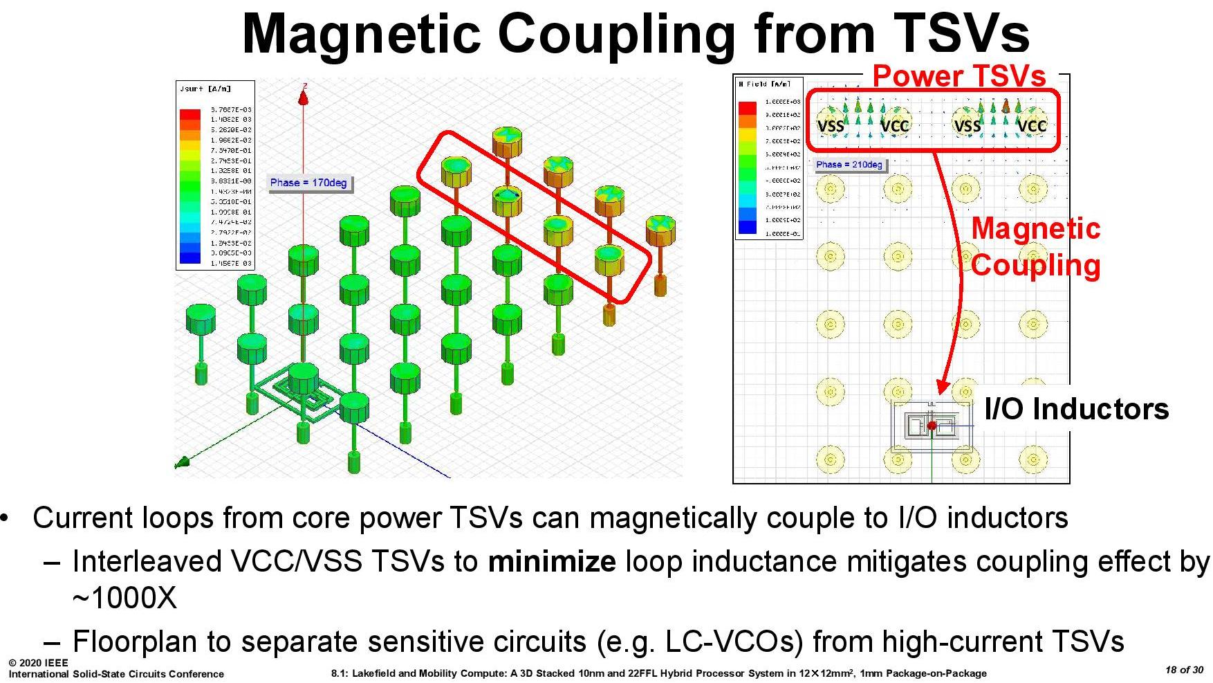
From this slide we can see that the simulations on TSVs in the base die required different types of TSV to be interleaved in order to minimize different electrical effects. High current TSVs are very clearly given the widest berth in the design.
When it comes to the IO of the bottom die, users might see that PCIe 3.0 designation and baulk – here would be a prime opportunity for Intel to announce a PCIe 4.0 product, especially with a separate focused IO silicon chiplet design. However, Lakefield isn’t a processor that is going to be paired with a discrete GPU, and these PCIe lanes are meant for additional peripherals, such as a smartphone modem.
Not to be discouraged, Intel has presented that it has looked into high-speed IO through its die-to-die interconnect.
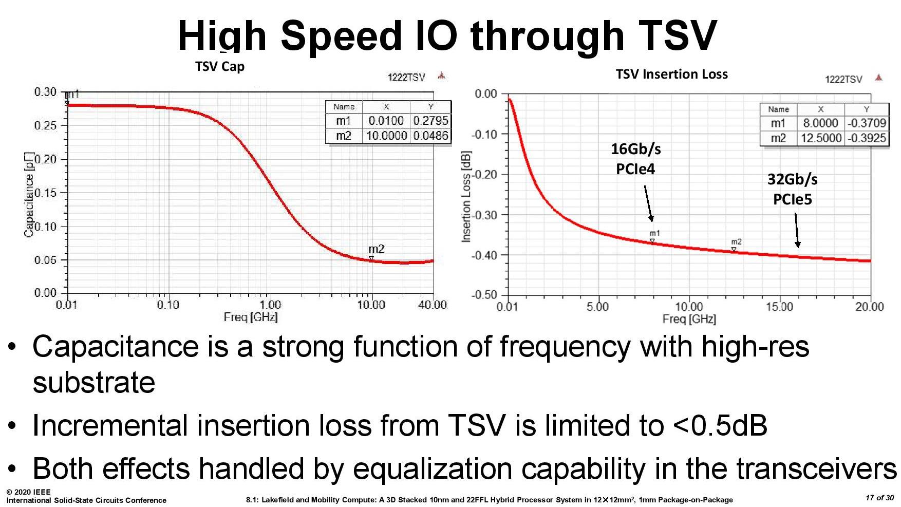
In this case, Intel battles capacitance as the higher frequency requirements of newer PCIe specifications. In this instance the signal insertion loss difference between PCIe 4.0 and PCIe 5.0 is fairly low, and well within a 0.5 dB variance. This means that this sort of connectivity might see its way into future products.
Memory
Also built into the package is the onboard memory – in this case it is DRAM, not any form of additional cache. The PoP memory on top (PoP stands for Package on Package) comes from a third party, and Intel assembles this at manufacturing before the product is sold to its partners. Intel will offer Lakefield with 8 GB and 4 GB variants, both built on some fast LPDDR4X-4266 memory.
In our conversations with Intel, the company steadfastly refuses to disclose who is producing the memory, and will only confirm it is not Intel. It would appear that the memory for Lakefield is likely a custom part specifically for Intel. We will have to wait until some of our peers take the strong acids to a Lakefield CPU in order to find out exactly who is working with Intel (or Intel could just tell us).
The total height, including DRAM, should be 1 mm.
As mentioned earlier in the article, Intel moving to chiplets one on top of the other exchanges the tradeoff of package size for one of cooling, especially when putting two computationally active parts of silicon together and then a big hunk of DRAM on top. Next we’ll consider some of the thermal aspects to Lakefield.


221 Comments
View All Comments
ProDigit - Friday, July 3, 2020 - link
It actually starts making sense, once you start doubling up on the cores. Sure, dual or quad core atom processors aren't really a thing. But at 95W tdp, you could be running a 30 to 60 core cpu. And those numbers are for 14nm. Not 10.That could make it interesting!
Alexvrb - Saturday, July 4, 2020 - link
Heck toss in 200W of these and it can be used to generate polygons and stuff! Oh wait... they already tried that. Seriously, a pile of slower cores might be OK for a secondary chip (accelerator) but it's not ideal for a main CPU and even less so for a consumer use case. Even a fast quad core would beat the stuffing out of a 60 core Atom for the overwhelming majority of consumer workloads.Actually, even as an accelerator for professional use there are often better solutions - GPUs and/or purpose-built accelerators, depending on your workload. That's why Intel shifted gears in that realm too.
LiKenun - Thursday, July 2, 2020 - link
The way I understand the implications for programmers… sometimes a program will do a one-time check for a particular processor feature (e.g.: if Avx2.IsSupported == true) and load optimized code at startup or optimize byte code compilation to remove unused branches. Then the program uses the loaded implementations for its entire running lifetime. There’s going to be a lot of work needed to undo these assumptions about processor feature sets not changing while the program is running.Lucky Stripes 99 - Saturday, July 4, 2020 - link
It would really be nice if Windows became better about ISA and API version controls. Instead of having to do a bunch of run time checks to avoid arcane system errors, I'd like to be able to set some minimum versions in the header of the EXE so that things will gracefully fail at startup. From a scheduler standpoint, this could allow you to have cores with different ISA versions and it would know which cores to avoid.ProDigit - Friday, July 3, 2020 - link
Yeah? Tell me where you can actually use avx512 or avx2? Most home users don't need it. Intel makes chips for businesses and for most home users.Not for those that occasionally need to run programs that are made for servers or performance machines.
Avx2/512 makes no sense, and has no home in a laptop.
Cullinaire - Friday, July 3, 2020 - link
Don't mind him, he's always harping about avx512 every chance he gets even though it's pointless.lefty2 - Friday, July 3, 2020 - link
Yes, home users do need it. AVX512 is rarely used, but AVX2 is almost universal.eastcoast_pete - Friday, July 3, 2020 - link
So, I guess you don't use Microsoft Teams or other video conferencing software on your laptop? Because those use AVX or AVX2 for virtual backgrounds, amongst other features.Regarding "no place in laptops", I vaguely remember hearing that about SSEs way back.
dotjaz - Saturday, July 4, 2020 - link
Well, AVX512 is truly pointless on a laptop, and possibly on any general consumer parts. That much is true. It is not energy efficient at all. On top of that, there's the mess of subsets.But AVX2 does provide sizable benefits over SSE4 even for optimal code. AVX alone is probably not worth it.
eastcoast_pete - Sunday, July 5, 2020 - link
With regard to AVX512, it's also a chicken-or-egg issue; as long as software makers can (correctly) assume that most of their customers don't have CPUs that have it, they won't use it, even where it would speed things up over AVX2. That's why AMD starting to have their own implementation of AVX512 is so important; it'll make it more of a mainstream feature that programmers can assume to be available for use by their software. That's one of the reasons this boneheaded move by Intel ticks me off.