Intel Next-Gen 10-micron Stacking: Going 3D Beyond Foveros
by Dr. Ian Cutress on August 14, 2020 2:30 PM EST_678x452.jpg)
One of the issues facing next-generation 3D stacking of chips is how to increase the density of the die-to-die interface. More connections means better data throughput, reducing latency and increasing bandwidth between two active areas of silicon that might be manufactured at different process nodes. There’s also a consideration for power and thermal hotspots as well. Intel has been developing its own physical interconnect topologies, most of which we’ve covered in detail before, such as the Embedded Multi-Die Interconnect Bridge (EMIB) that allows 2D expansion and Foveros die-to-die 3D staking that enables vertical expansion. As part of Intel’s Architecture Day 2020, we have a glimpse into Intel’s future with hybrid bonding.
There are several holistic metrics to measure how ‘good’ an interconnect can be; the two that are easiest to understand are density of connections (bump density) and energy (how much energy it takes to transfer a bit).
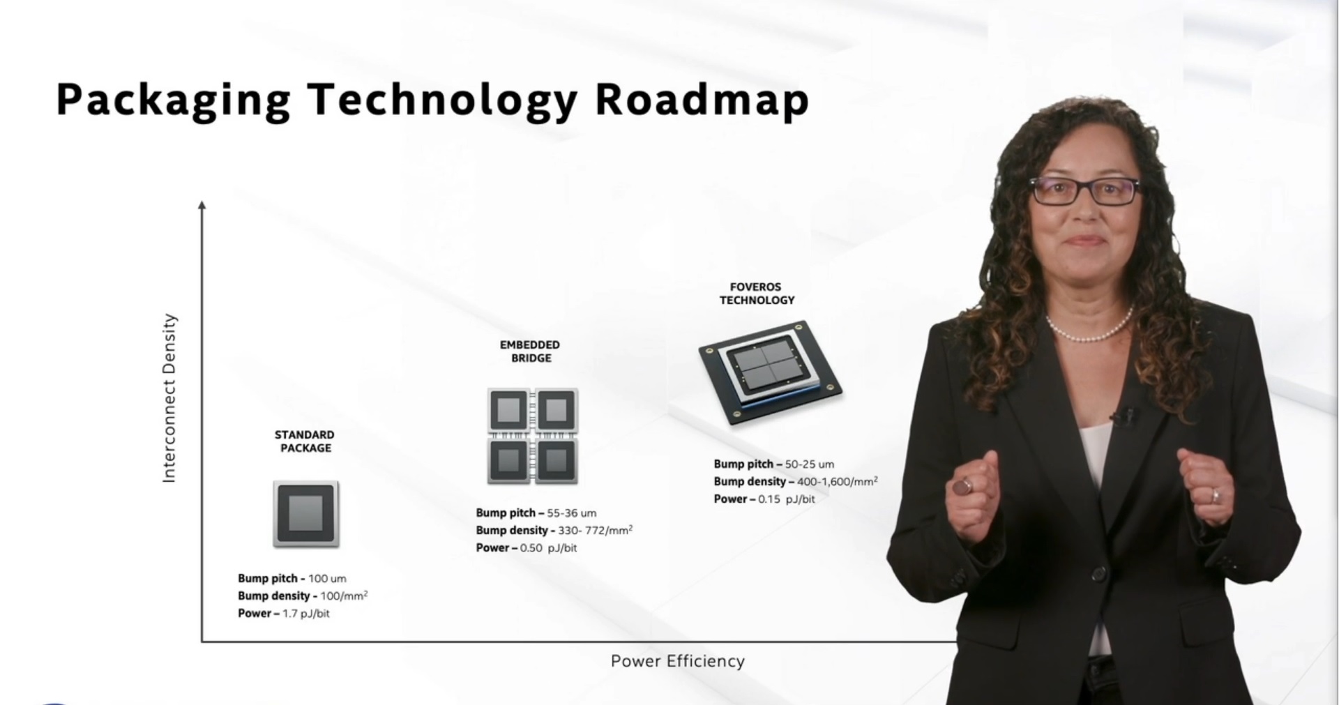
Intel's Ramune Nagisetty showcasing current packaging technologies at Intel
Intel’s own slides show us that EMIB’s bump density is good for ~400 per square millimeter, with a power of 0.50 picojoules per bit transferred. Foveros takes that a step further, supporting 400-1600 bumps per square millimeter, and an average power of 0.15 picojoules per bit transferred.
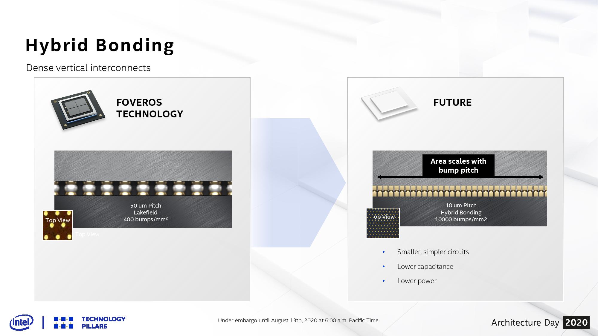
The next era of ‘Hybrid Bonding’ that Intel is going towards improves both metrics by around a factor of 3-10. The new test chips that Intel has just got back into the lab, involving stacked SRAM, goes towards the 10000 bumps per square millimeter range, with a power under 0.05 picojoules per bit. According to Intel this allows for smaller and simpler circuits, with lower capacitance and better efficiency. Nothing to be said about yields however!
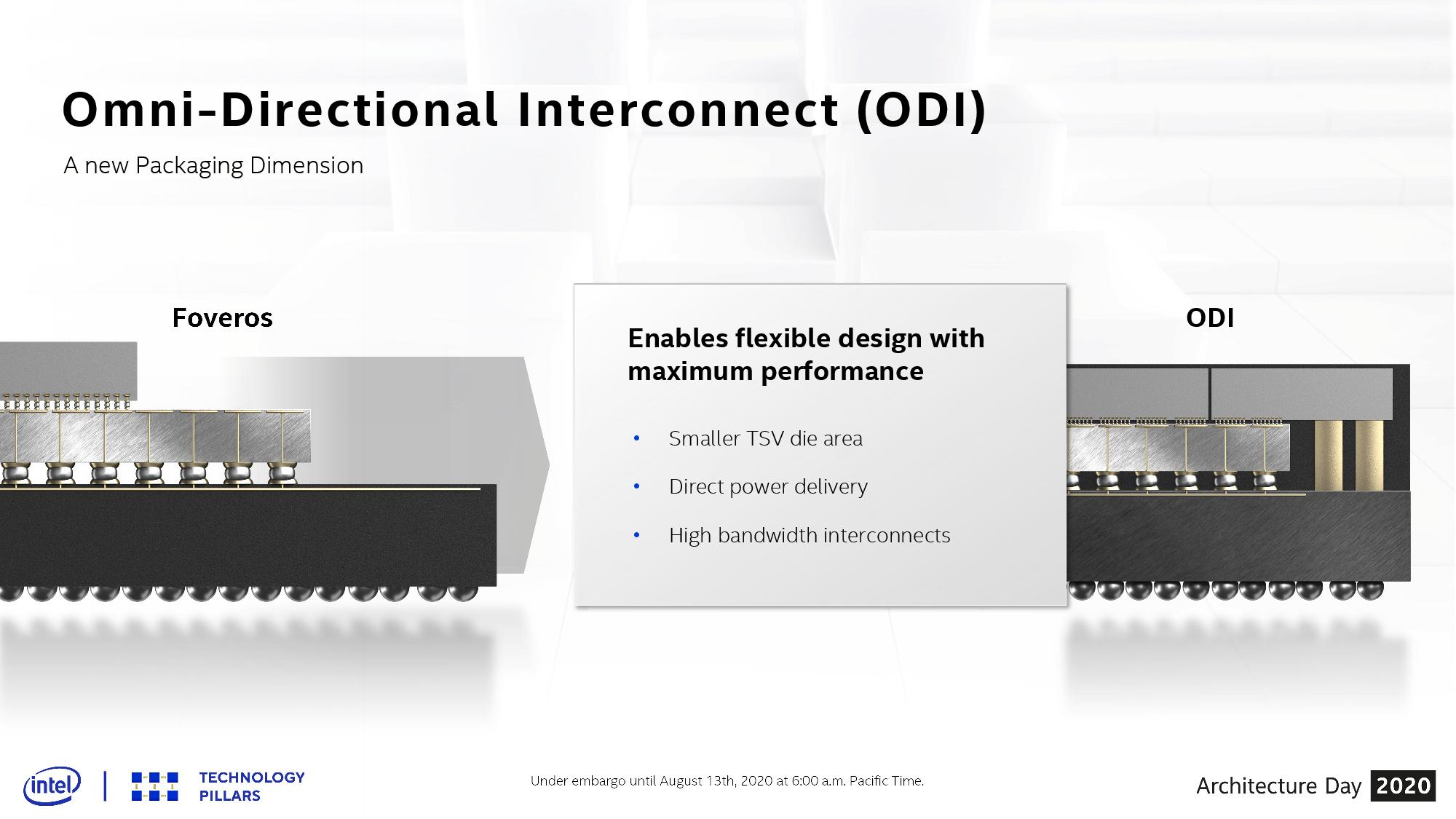
With these new bonding and stacking technologies, the question always becomes one of thermals, and how Intel might stack two performance-related bits of silicon together. In the discussions as part of Architecture Day, Intel stated that these stacked designs require having all layers designed together, rather than independently, in order to manage the electrical and thermal characteristics. As far as Intel sees it, the most power hungry layer is required to go on the top of the stack for the time being, which obviously means that the power connections have to either rise up through the lower layers, or there has to be some form of cantilevered situation where power connections can happen off the edge of the bonding – Intel calls this technology ODI, to support different sized silicon layers.
With the future of high performance and high efficiency computing coming to a head with new packaging technologies, finding the right way of going forward is ever critical. For a context on timeline, Intel’s Ramune Nagisetty has stated that Foveros was patented back in 2008, but it took nearly a decade for the process to become physically viable at scale and high-enough yielding for a product to come to market.
Related Reading
- An Interconnected Interview with Intel’s Ramune Nagisetty: A Future with Foveros
- Intel: Lakefield in 2020, Possible 5G on Foveros
- Intel’s Xe for HPC: Ponte Vecchio with Chiplets, EMIB, and Foveros on 7nm, Coming 2021
- Hot Chips 31 Live Blogs: Intel Lakefield and Foveros
- Intel's Interconnected Future: Combining Chiplets, EMIB, and Foveros
- The Intel Lakefield Deep Dive: Everything To Know About the First x86 Hybrid CPU

_thumb.jpg)
_575px_thumb.jpg)
_carousel_thumb.jpg)
_carousel_thumb.jpg)
_thumb.jpg)


31 Comments
View All Comments
DanNeely - Monday, August 17, 2020 - link
No, just assuming that it's going to be expensive initially which means it'll be used in high end server chips at first (where the socket is huge for IO anyway, and can be made larger as needed without major issues) and not trickle down to size sensitive laptop parts for several more years.Santoval - Saturday, August 15, 2020 - link
"and they've still got Foveros to do horizontal connections similar to AMD chiplets"You rather meant "they've still got *EMIB*" right?
Spunjji - Monday, August 17, 2020 - link
That could be a pretty sweet way to do things. It does sound expensive, though...rahvin - Friday, August 14, 2020 - link
Every single diagram I've seen stacks the CPU on the bottom with memory and other layers on top. All that CPU heat then has to move through each additional layer to cool the CPU including heating the cache layers up to the point where it will affect memory performance requiring lower memory clocks etc.I get that the intent is to boost bandwidth to the CPU but the heat issue IMO negates that much of that benefit. It will be interesting if they can get the tech working and can produce at volume without a huge financial cost but frankly I think it's dead end tech for general CPU's. Maybe it has value in other applications but concentrating heat in smaller form factors IMO is never going to be a winning strategy.
coburn_c - Friday, August 14, 2020 - link
Flip. Chip.whatthe123 - Friday, August 14, 2020 - link
I mean it says right in the article "As far as Intel sees it, the most power hungry layer is required to go on the top of the stack for the time being."Valantar - Saturday, August 15, 2020 - link
That is the only logical solution, yes, however current solutions do exactly the opposite. Standard PoP packaging is even worse, with a significant air gap in there as well.DanNeely - Saturday, August 15, 2020 - link
That's because in standard pop, you've just got the two chips talking to each other; Intel's R&D has been about having the top chips connections go through the bottom chip to the PCB and delivering enough power to the top chip for high performance uses.Doing that lets them put high performance chips on top for optimal cooling; but it also means that the top and bottom chips are tightly coupled as a pair. That in turn means that POP isn't going anywhere in the mobile market; with the possible exception of Apple, no one is going to design a custom ram chip that can only work with their SoC (because it has all the connections to route the SoC to the mobo going through it).
JayNor - Saturday, August 15, 2020 - link
The Lakefield layers total 1mm thick. Is there a huge difference in temperature between top and bottom chiplets after the initial warm-up? Perhaps the new insulation material helps ...from a Wired article, "An Intel Breakthrough Rethinks How Chips Are Made":
"Koduri keeps the specifics of exactly how Intel cracked those problems closely held. But he says that a combination of rigorous testing, a new power delivery process, and a wholly invented insulation material to dissipate the heat has helped the company avoid the typical pitfalls."
c4v3man - Friday, August 14, 2020 - link
Not every design has to be focused on peak performance with infinite space/power. In something like a phone, thermals are limited by the chassis itself, so whether you have 150 square millimeters, or 50 square millimeters contacting the chassis, that makes little difference if the chassis can only dissipate 5 watts of power passively anyways. In that sort of installation, reducing power draw, and heat generation via interconnects is more important. Stacking has the potential to dramatically reduce this inefficiency/thermal waste, meaning of your 5 watts of cooling capacity goes even further. Not to mention packaging efficiency, allowing for larger batteries, etc.