Intel Next-Gen 10-micron Stacking: Going 3D Beyond Foveros
by Dr. Ian Cutress on August 14, 2020 2:30 PM EST_678x452.jpg)
One of the issues facing next-generation 3D stacking of chips is how to increase the density of the die-to-die interface. More connections means better data throughput, reducing latency and increasing bandwidth between two active areas of silicon that might be manufactured at different process nodes. There’s also a consideration for power and thermal hotspots as well. Intel has been developing its own physical interconnect topologies, most of which we’ve covered in detail before, such as the Embedded Multi-Die Interconnect Bridge (EMIB) that allows 2D expansion and Foveros die-to-die 3D staking that enables vertical expansion. As part of Intel’s Architecture Day 2020, we have a glimpse into Intel’s future with hybrid bonding.
There are several holistic metrics to measure how ‘good’ an interconnect can be; the two that are easiest to understand are density of connections (bump density) and energy (how much energy it takes to transfer a bit).
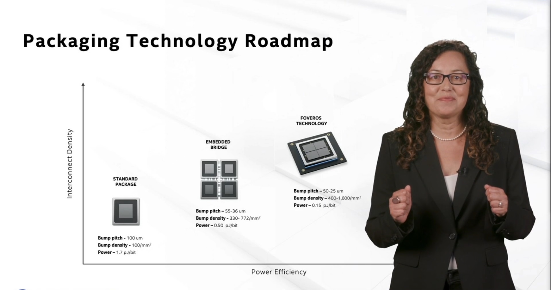
Intel's Ramune Nagisetty showcasing current packaging technologies at Intel
Intel’s own slides show us that EMIB’s bump density is good for ~400 per square millimeter, with a power of 0.50 picojoules per bit transferred. Foveros takes that a step further, supporting 400-1600 bumps per square millimeter, and an average power of 0.15 picojoules per bit transferred.
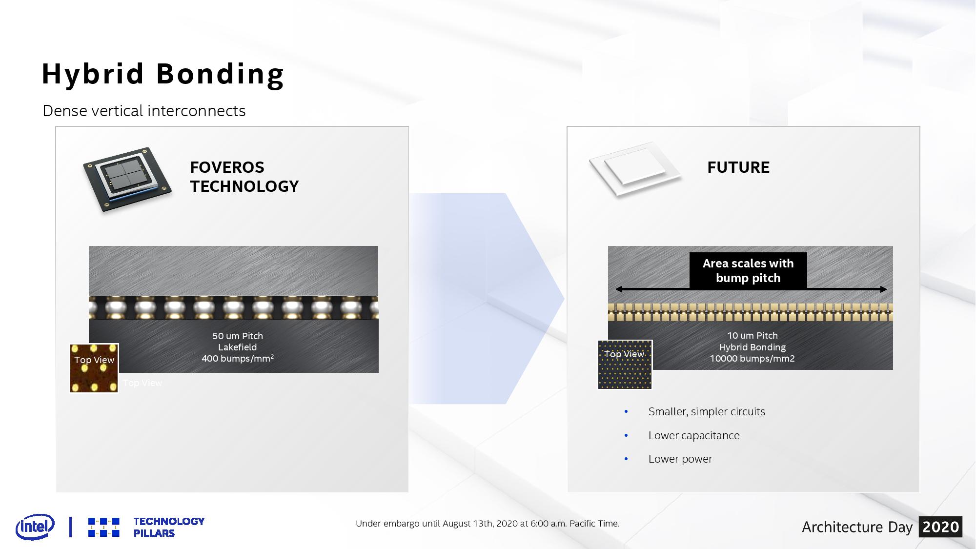
The next era of ‘Hybrid Bonding’ that Intel is going towards improves both metrics by around a factor of 3-10. The new test chips that Intel has just got back into the lab, involving stacked SRAM, goes towards the 10000 bumps per square millimeter range, with a power under 0.05 picojoules per bit. According to Intel this allows for smaller and simpler circuits, with lower capacitance and better efficiency. Nothing to be said about yields however!
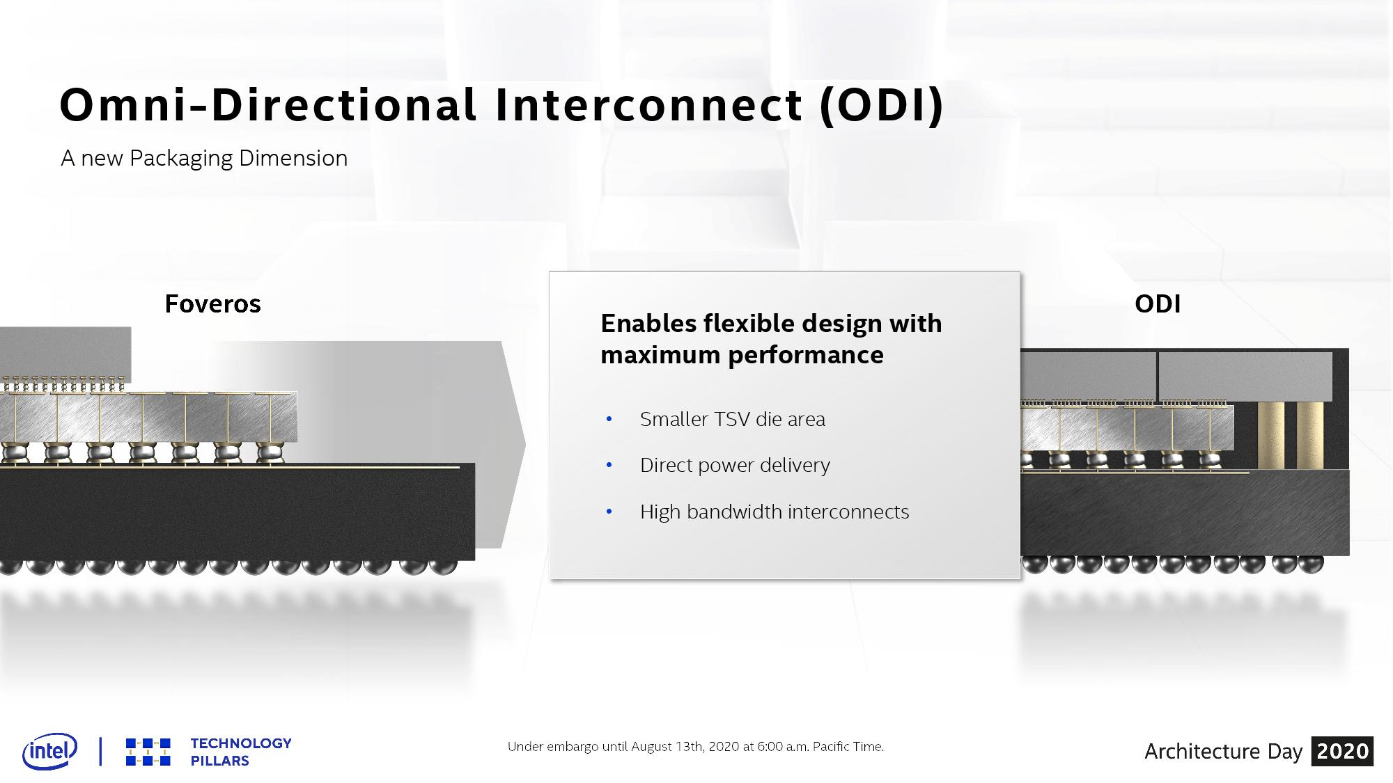
With these new bonding and stacking technologies, the question always becomes one of thermals, and how Intel might stack two performance-related bits of silicon together. In the discussions as part of Architecture Day, Intel stated that these stacked designs require having all layers designed together, rather than independently, in order to manage the electrical and thermal characteristics. As far as Intel sees it, the most power hungry layer is required to go on the top of the stack for the time being, which obviously means that the power connections have to either rise up through the lower layers, or there has to be some form of cantilevered situation where power connections can happen off the edge of the bonding – Intel calls this technology ODI, to support different sized silicon layers.
With the future of high performance and high efficiency computing coming to a head with new packaging technologies, finding the right way of going forward is ever critical. For a context on timeline, Intel’s Ramune Nagisetty has stated that Foveros was patented back in 2008, but it took nearly a decade for the process to become physically viable at scale and high-enough yielding for a product to come to market.
Related Reading
- An Interconnected Interview with Intel’s Ramune Nagisetty: A Future with Foveros
- Intel: Lakefield in 2020, Possible 5G on Foveros
- Intel’s Xe for HPC: Ponte Vecchio with Chiplets, EMIB, and Foveros on 7nm, Coming 2021
- Hot Chips 31 Live Blogs: Intel Lakefield and Foveros
- Intel's Interconnected Future: Combining Chiplets, EMIB, and Foveros
- The Intel Lakefield Deep Dive: Everything To Know About the First x86 Hybrid CPU

_thumb.jpg)
_575px_thumb.jpg)
_carousel_thumb.jpg)
_carousel_thumb.jpg)
_thumb.jpg)


31 Comments
View All Comments
Duncan Macdonald - Friday, August 14, 2020 - link
Intel lost the phone (and other low power devices) market to ARM years ago, Intel's CPUs are all in the >5W range (most >20W) for which cooling is a major design consideration. At the Ultrabook level (<15W) stacking one layer above the CPU might be tolerable, going beyond this into high performance CPUs and/or multiple layers above the CPU is very questionable.lmcd - Friday, August 14, 2020 - link
Intel's Atom designs idle in the same range as ARM and ARM peak consumption keeps creeping closer to Intel. Also, you're delusional if you think Intel is counting itself out of phones forever. The MediaTek partnership, just for connected laptops? No.Spunjji - Monday, August 17, 2020 - link
I'd be interested in your evidence for that first claim. They never *did* idle particularly close to ARM, and I'm not aware of a current direct comparison that could be made because we've still not seen the numbers for Lakefield.nandnandnand - Friday, August 14, 2020 - link
Stacking is the future, and AMD will be doing it too:https://www.anandtech.com/show/15590/amd-discusses...
Getting memory closer to logic can lower power consumption and heat.
FaaR - Friday, August 14, 2020 - link
It lowers total heat yes, but as mentioned, it can also create local hotspots, which is problematic.JayNor - Saturday, August 15, 2020 - link
Intel is building 144 layer NAND chips.They don't have to use many chiplet layers to get the benefits of layering logic. For example, Lakefield uses an ultra low leakage 22FL IO bottom layer, with the compute layer on top of it and with the two layers of DDR sitting on top.
I could easily see a Lakefield stack expanded outward to more cores and IO. Perhaps add in a couple of internal layers for L3 cache to reduce the area even more. Perhaps put the Gracemont cores on a layer of their own in the coming Alder Lake.
name99 - Saturday, August 15, 2020 - link
It's only a dead end if you prioritize GHz over every other aspect of your design...So yeah, Intel's in a crazy spot with the left hand not knowing what the right hand is doing. But for everyone else, the sorts of people using eg https://www.tsmc.com/english/dedicatedFoundry/tech...
it's rather less of an issue.
We already have various versions of stacking in the mobile world -- the obvious PoP, the newer InFO used by iPhones for a while now,
https://www.systemplus.fr/wp-content/uploads/2018/...
and the strange A12X hybrid
https://sst.semiconductor-digest.com/chipworks_rea...
Of course those are DRAM and logic, not stacked SRAM (ala Samsung) or logic on logic. But mainly that reflects the fact that Apple's current SoCs are small (so don't need to be made of multiple pieces) and TSMC's process can yield a 150mm^2 die without breaking a sweat. It will be interesting to see what geometries Apple uses for this as they want to go to larger logic.
surt - Saturday, August 15, 2020 - link
Given that cube is the most practical solid shape to manufacture with a high SA/V ratio (for heat dissipation), cube shaped chips via stacking seems the inevitable destination for CPU manufacturing.Santoval - Saturday, August 15, 2020 - link
3D stacking will never be achieved with packages above 15W, maybe 20W tops (with a robust -and non thin- cooling solution, which however would take space and thus largely negate the area savings of stacking everything on a single package), without some form of active cooling between the dies. Lakefield has a mere 7W TDP and is already thermally constrained.Microfluidic active cooling solutions have been tested in many labs for quite a few years now, but I doubt they are anywhere near ready to enter the market - unless the industry surprises us that is. Without them the TDP upper cap of 3D stacked SoCs should be in the ~15W range, with momentary TDP spikes of ~5W above that for the turbo clocks. Even then, a robust solution of combined active and passive cooling would be required, so these laptops would clearly not be silent.
They would also get *hot*, quite hotter* than the current setup of distinct SoCs and RAM, since all the heat that was previously coming from tens of square cm would be coming from just ~1 cm², in a much "denser" form.
* Technically they would be just as hot, but they would have a far higher thermal density, so it would feel like they were hotter at a particular spot, unless that heat was dissipated effectively.
FunBunny2 - Saturday, August 15, 2020 - link
"Microfluidic active cooling solutions"IBM did that 40 years, albeit at a macro level: https://www.ibm.com/ibm/history/exhibits/vintage/v...