Hot Chips 2020 Live Blog: Intel's Xe GPU Architecture (5:30pm PT)
by Dr. Ian Cutress on August 17, 2020 8:30 PM EST- Posted in
- GPUs
- Intel
- Live Blog
- Xe
- Hot Chips 32

08:37PM EDT - Intel's Xe talk, by David Blythe
08:37PM EDT - David did the Intel Architecture Xe talk

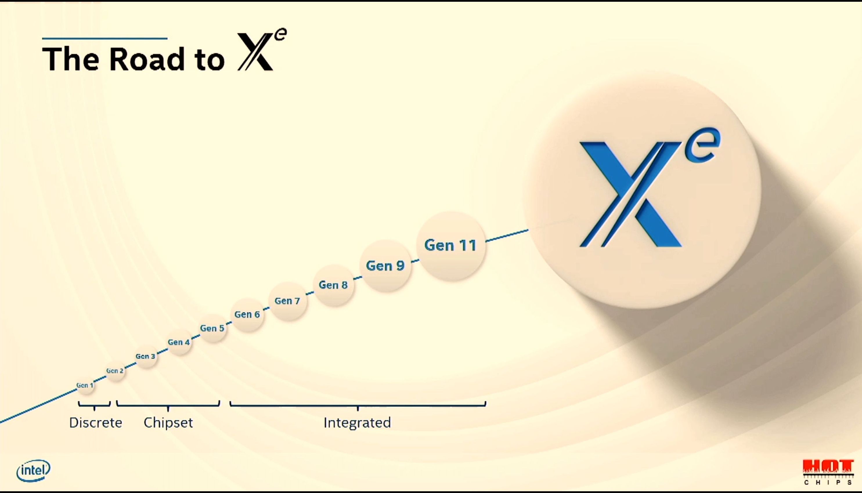
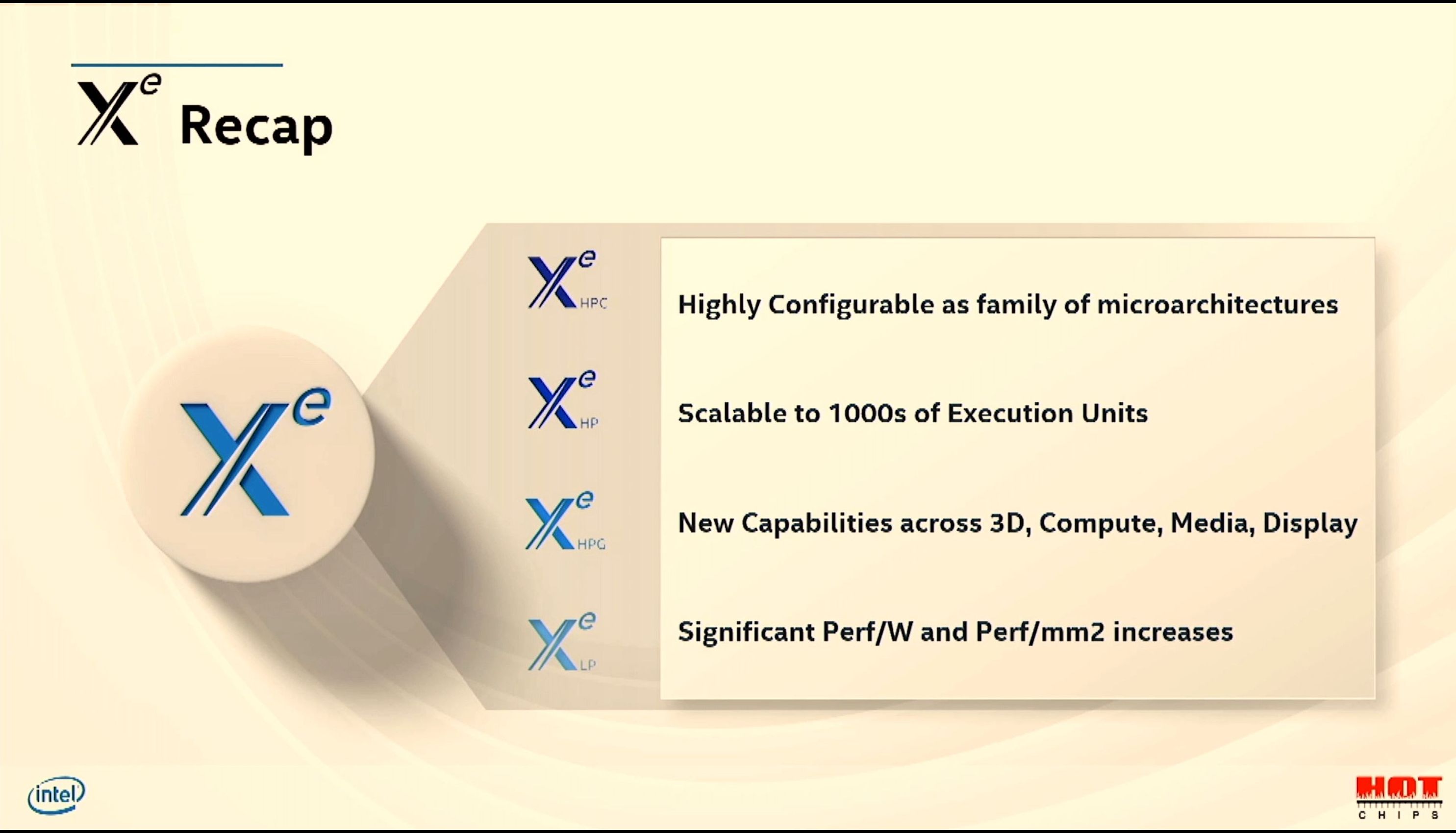
08:38PM EDT - Going forward in architecture than previously covered by integrated GPU
08:38PM EDT - Moving from Gen to Xe -> exascale for everyone
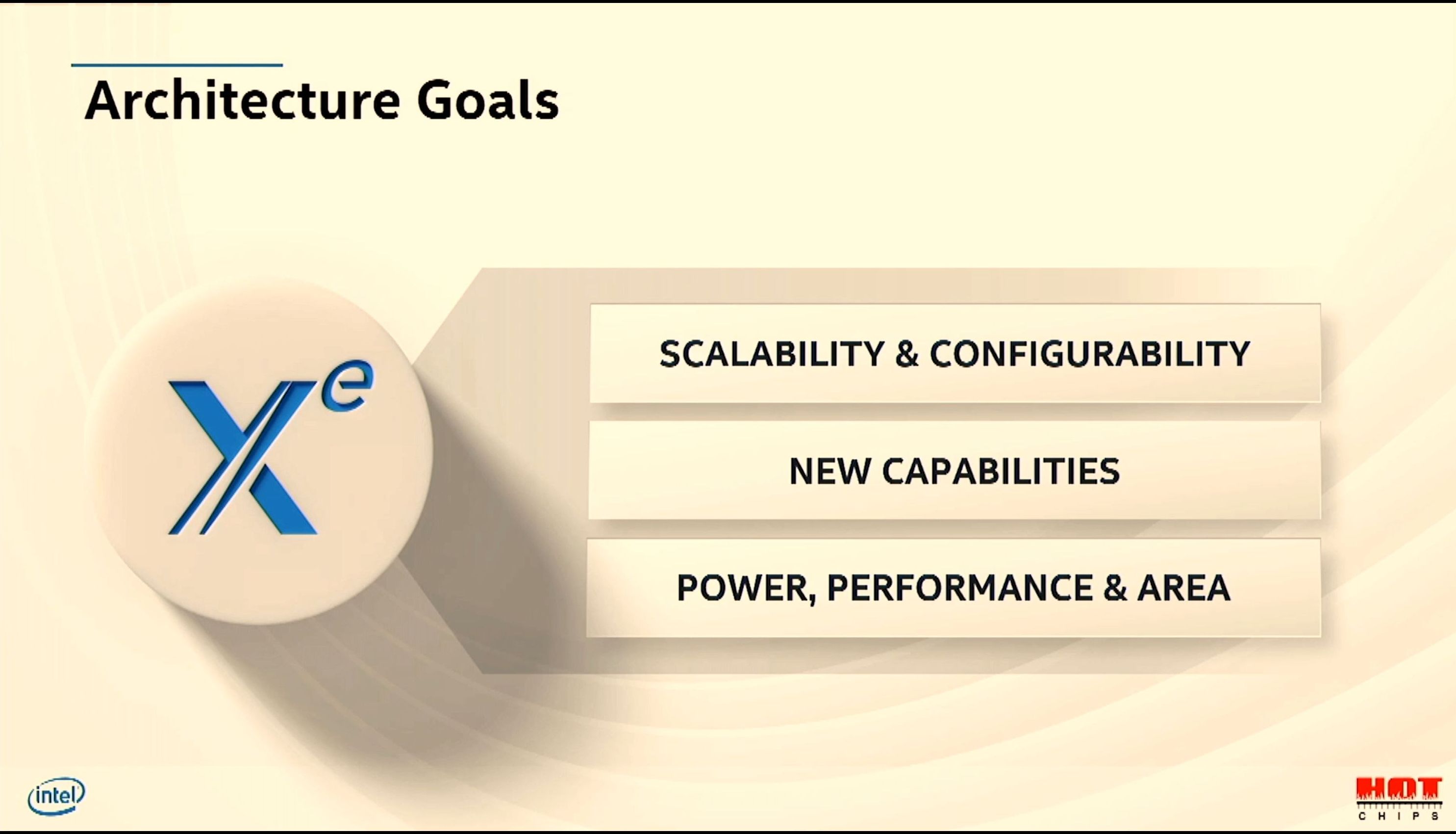
08:38PM EDT - Goals: increase SIMD lanes from 10s to 1000s
08:38PM EDT - Add new capabilities - matrix tensors, ray tracing, virtualization, etc
08:38PM EDT - Also PPA improvements
08:39PM EDT - Required a lot of new design over Gen11
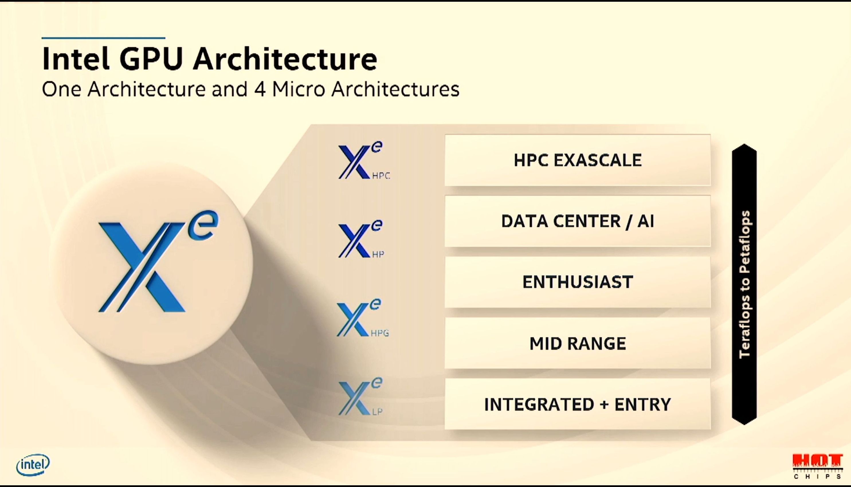
08:39PM EDT - Xe will scale from LP to HPG, HP, HPC
08:39PM EDT - Optimized for different market requirements
08:40PM EDT - Going beyond just adding execution units - but optimizing each segment with individual requirements
08:40PM EDT - Such as ray tracing, media, FP64 etc
08:40PM EDT - LP is integrated and entry
08:40PM EDT - HPG is Mid-range and Enthusiast
08:40PM EDT - HP is Datacenter and AI
08:40PM EDT - HPC is exascale
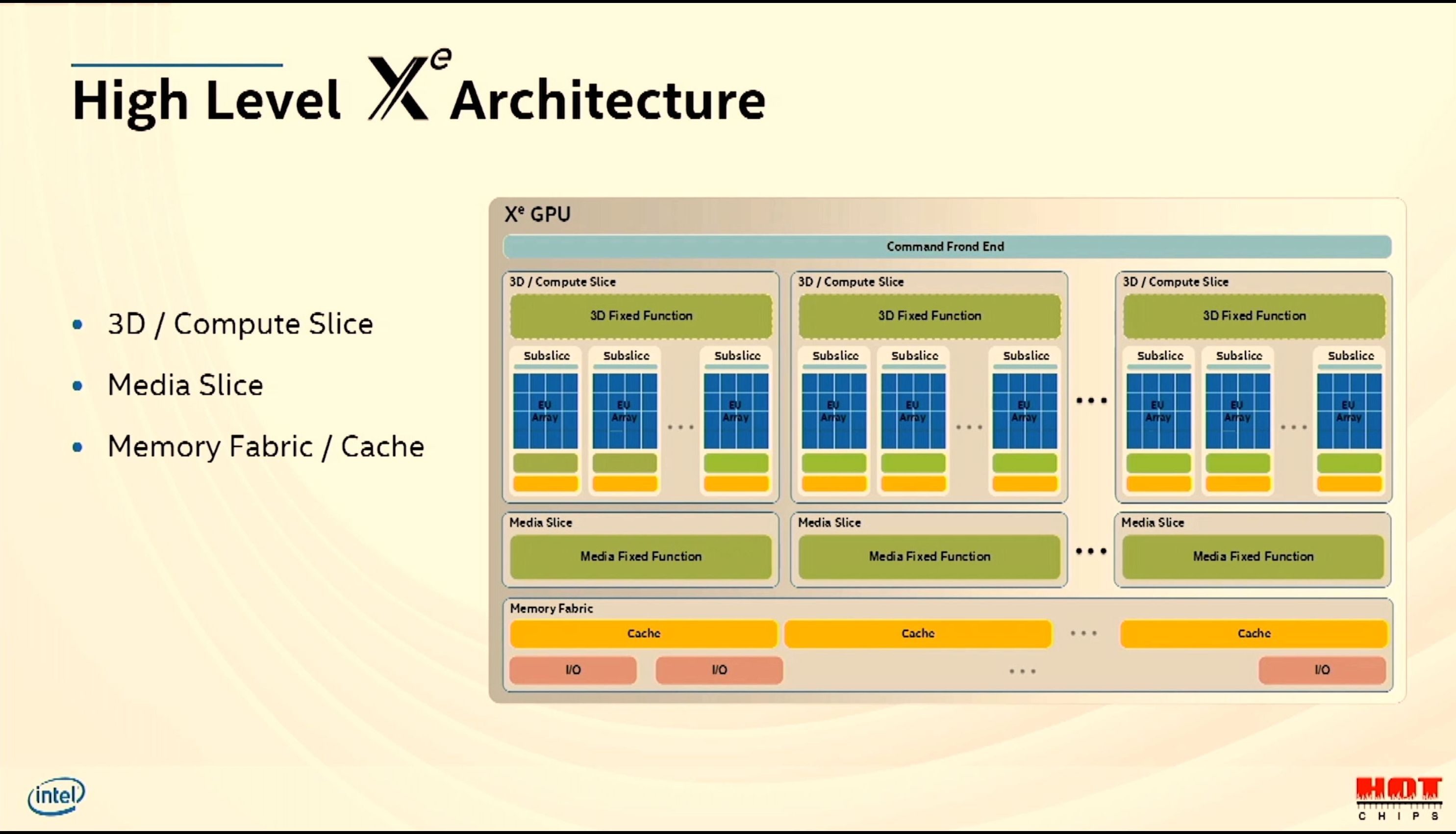
08:41PM EDT - There is a high-level Xe architecture
08:41PM EDT - 3D/Compute slice, media slice, memory fabric
08:41PM EDT - Each slice has sub-slices
08:41PM EDT - programmable shaders
08:41PM EDT - (Each compute slice is 96 EUs)
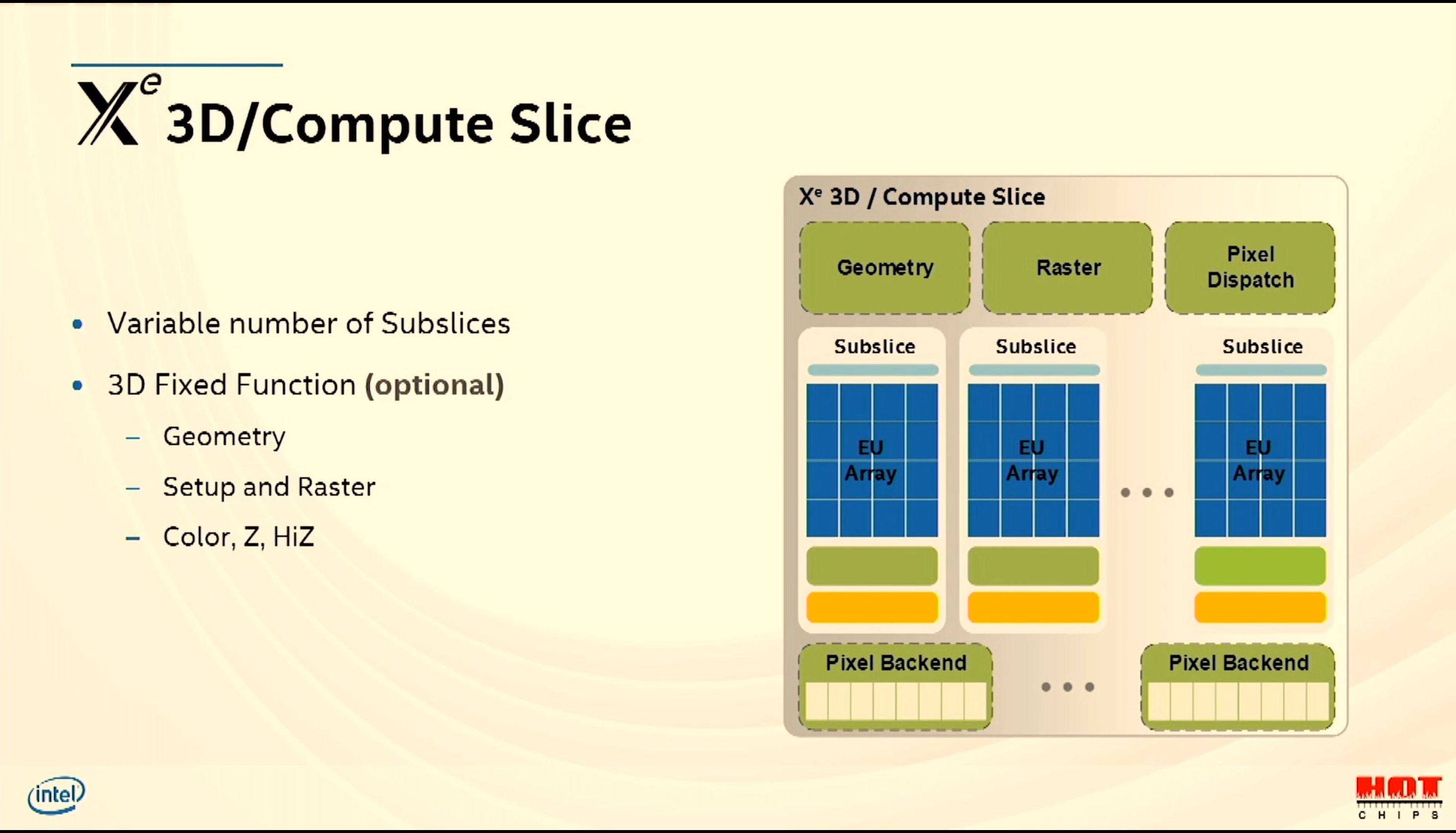
08:42PM EDT - Geometry has moved inside the slice and now distributed
08:42PM EDT - Slice size is adjustable
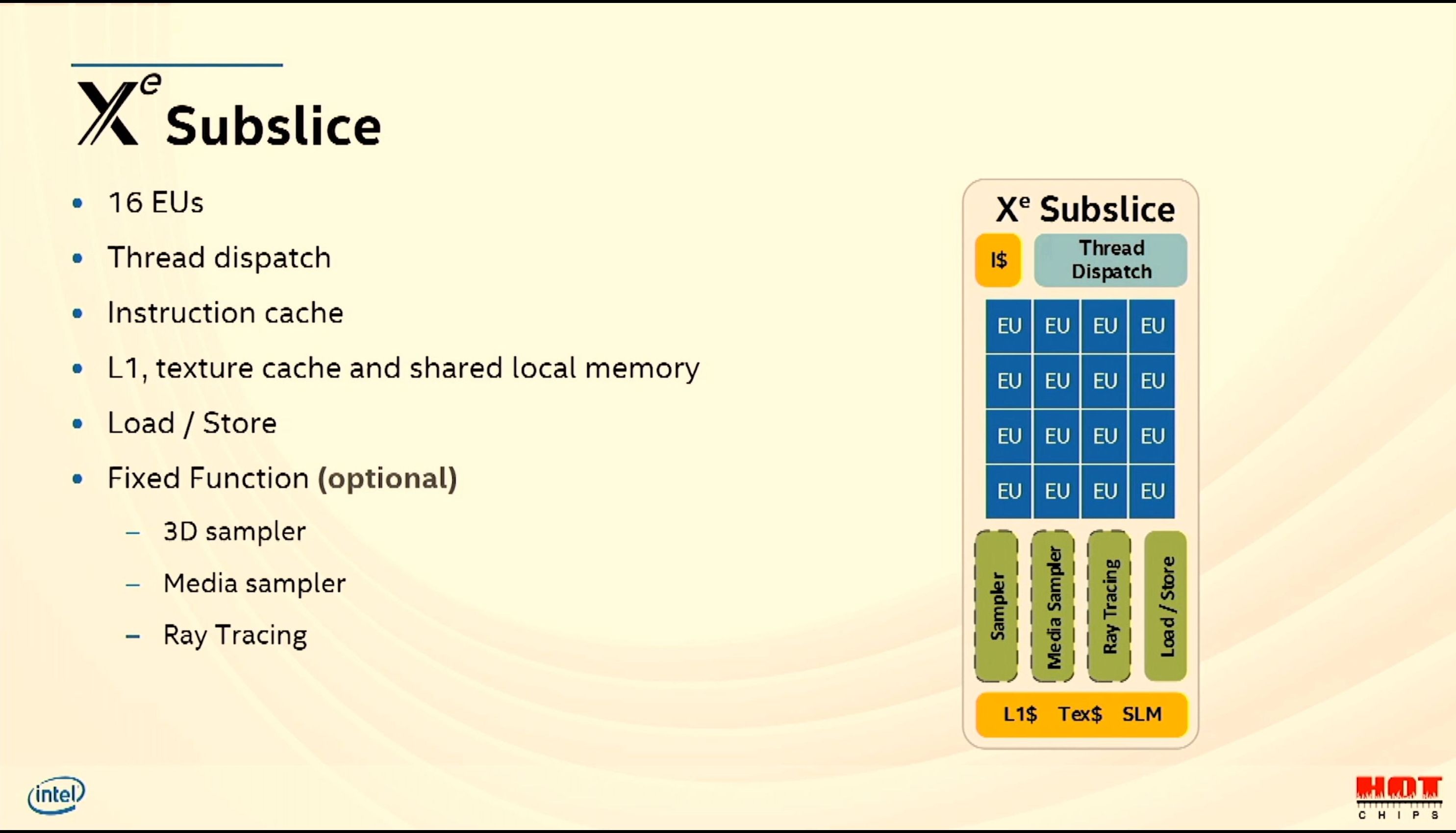
08:42PM EDT - Sub-slice has 16 EUs
08:42PM EDT - Fixed function units (optional based on segment)
08:42PM EDT - 16 EUs = 128 SIMD lanes
08:43PM EDT - hardware blocks for ray tracing
08:43PM EDT - XeHPG that uses Ray Tracing in the lab today
08:43PM EDT - L1 scratch pad

08:43PM EDT - Xe Execution Unit
08:44PM EDT - 8 INT/FP ports, 2 complex math
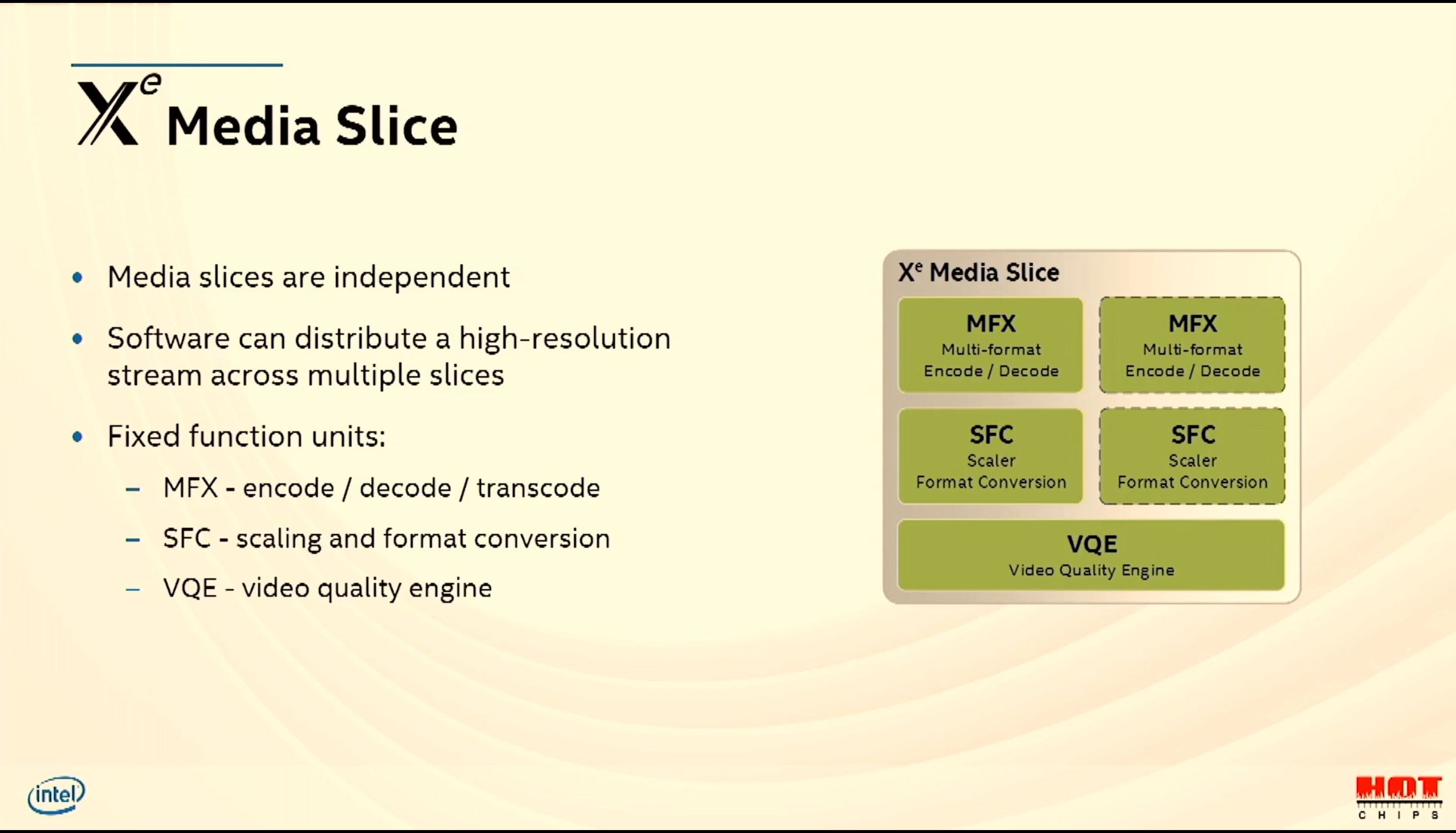
08:44PM EDT - Media processing can be scaled as well with media slices
08:44PM EDT - de-noise, de-interlace, tone mapping is all here
08:45PM EDT - can distribute a stream across mutiple slices

08:45PM EDT - Xe Memory Fabric
08:45PM EDT - L3 and Rambo cache
08:45PM EDT - Lots of optional stuff here
08:46PM EDT - Allows scaling to 1000 of EUs
08:46PM EDT - Requires multiple dies
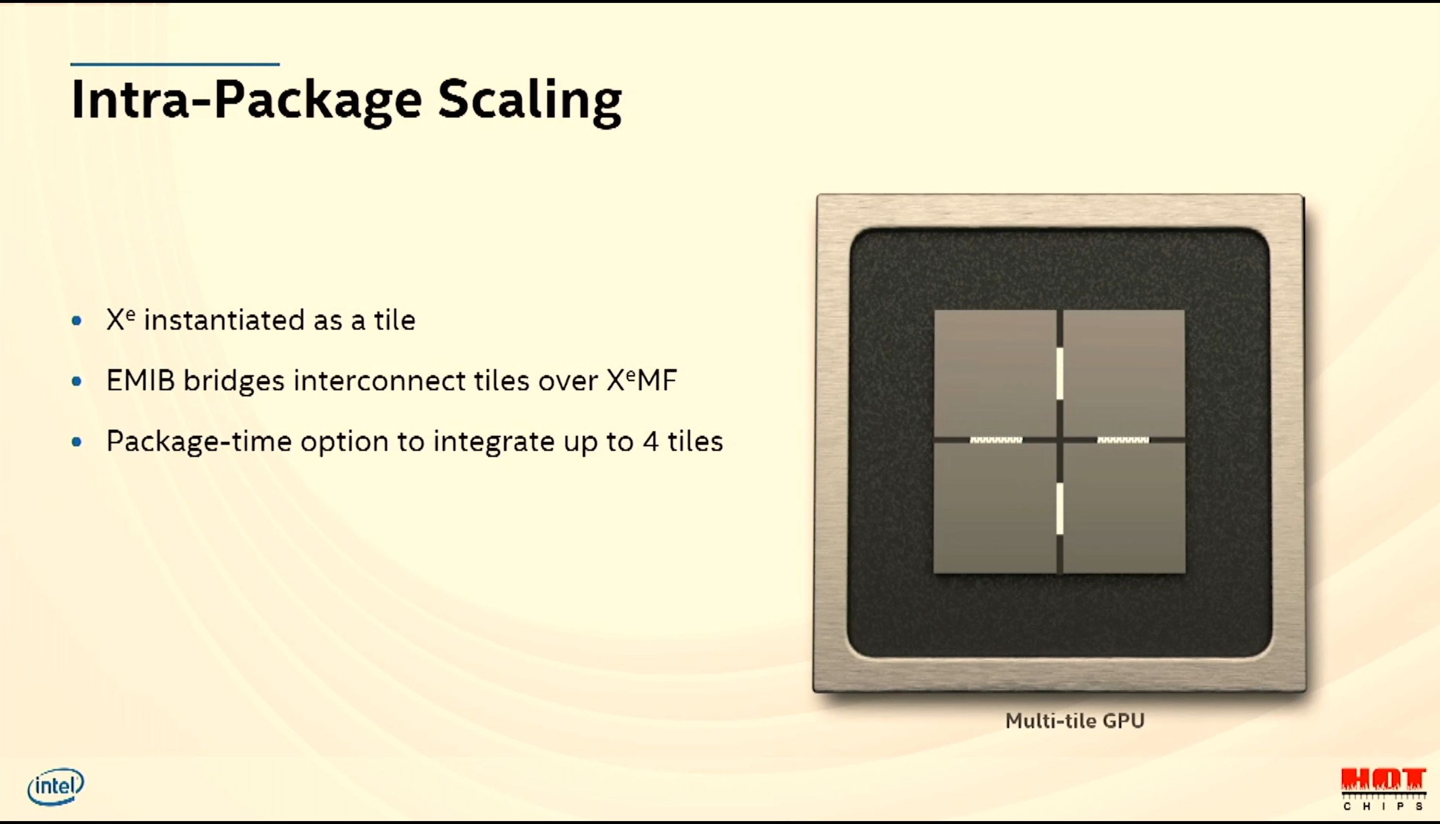
08:46PM EDT - Low level tile disaggregation
08:47PM EDT - Mutliple tiles work as separate GPUs or a single GPU
08:47PM EDT - EMIB does XeMF
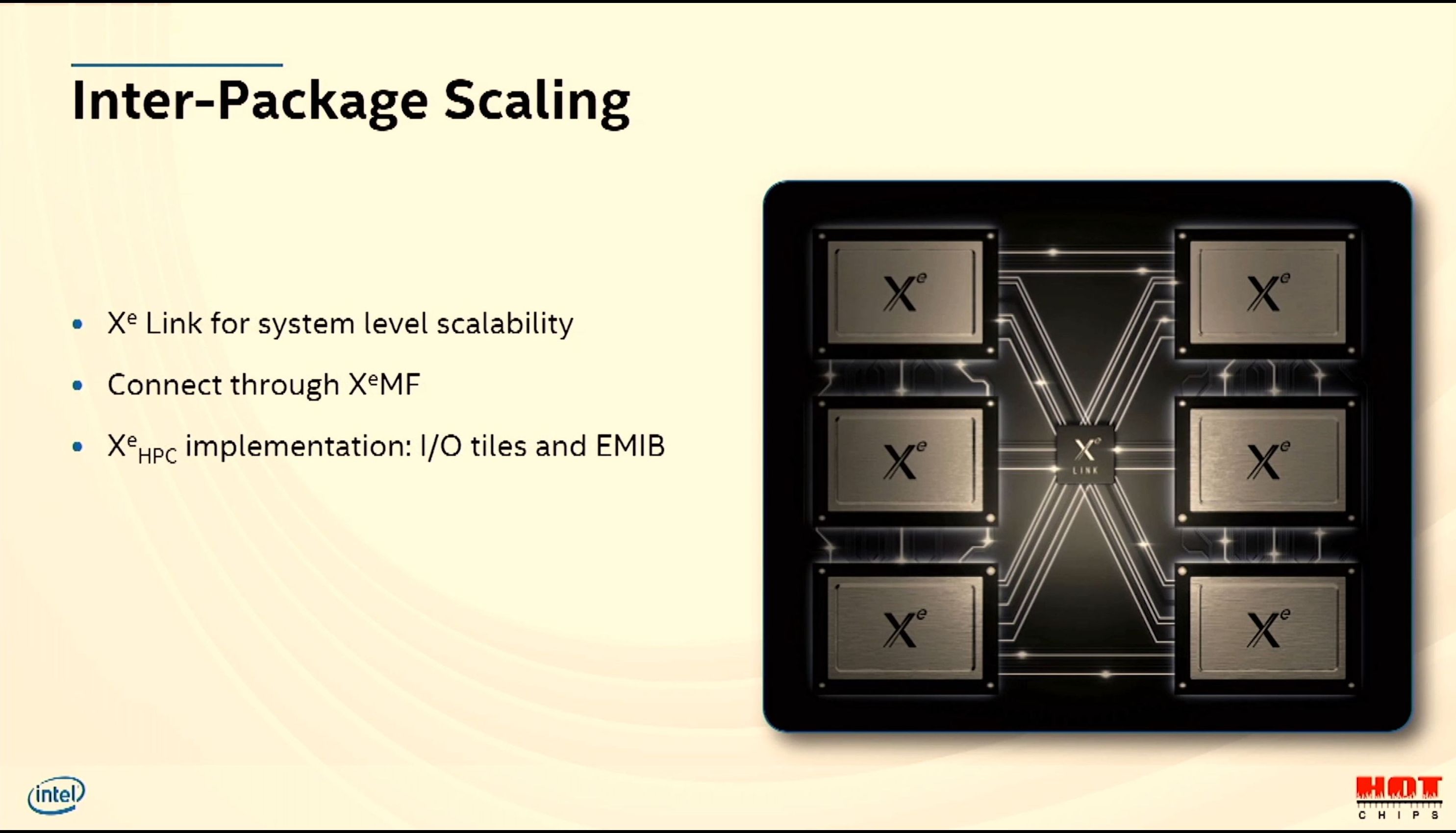
08:47PM EDT - Xe Link enables XeMF from GPU-to-GPU

08:48PM EDT - XeHP with HBM2e
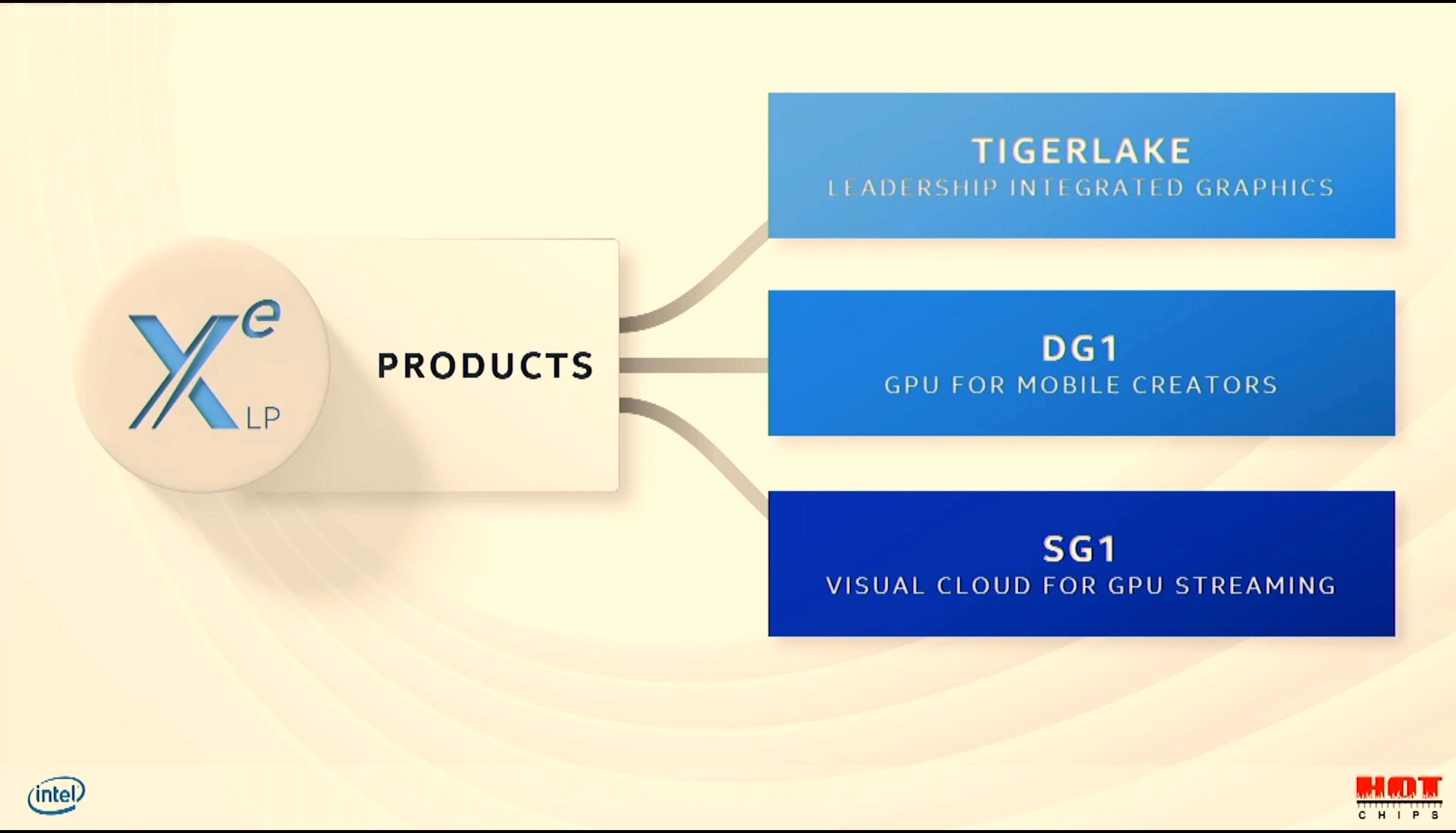
08:48PM EDT - XeLP is low power optimized
08:48PM EDT - Tiger Lake, SG1, and DG1 will all be XeLP
08:49PM EDT - Tiger Lake goal was to increase perf 2x in graphics
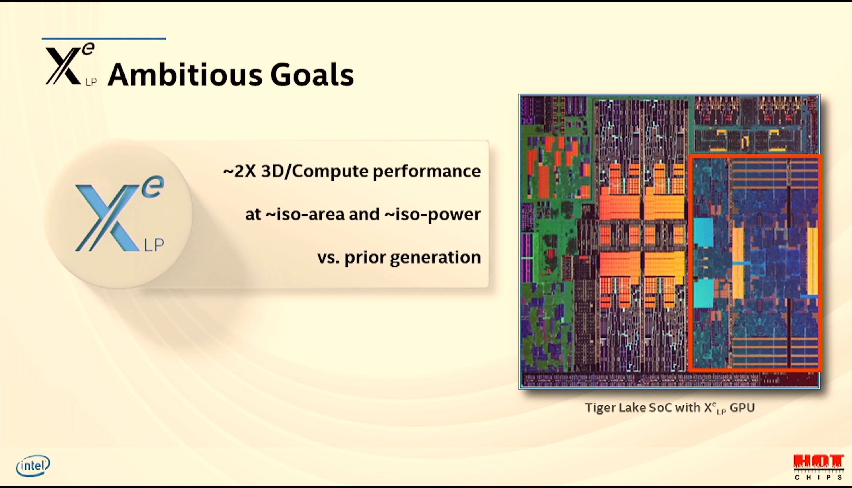
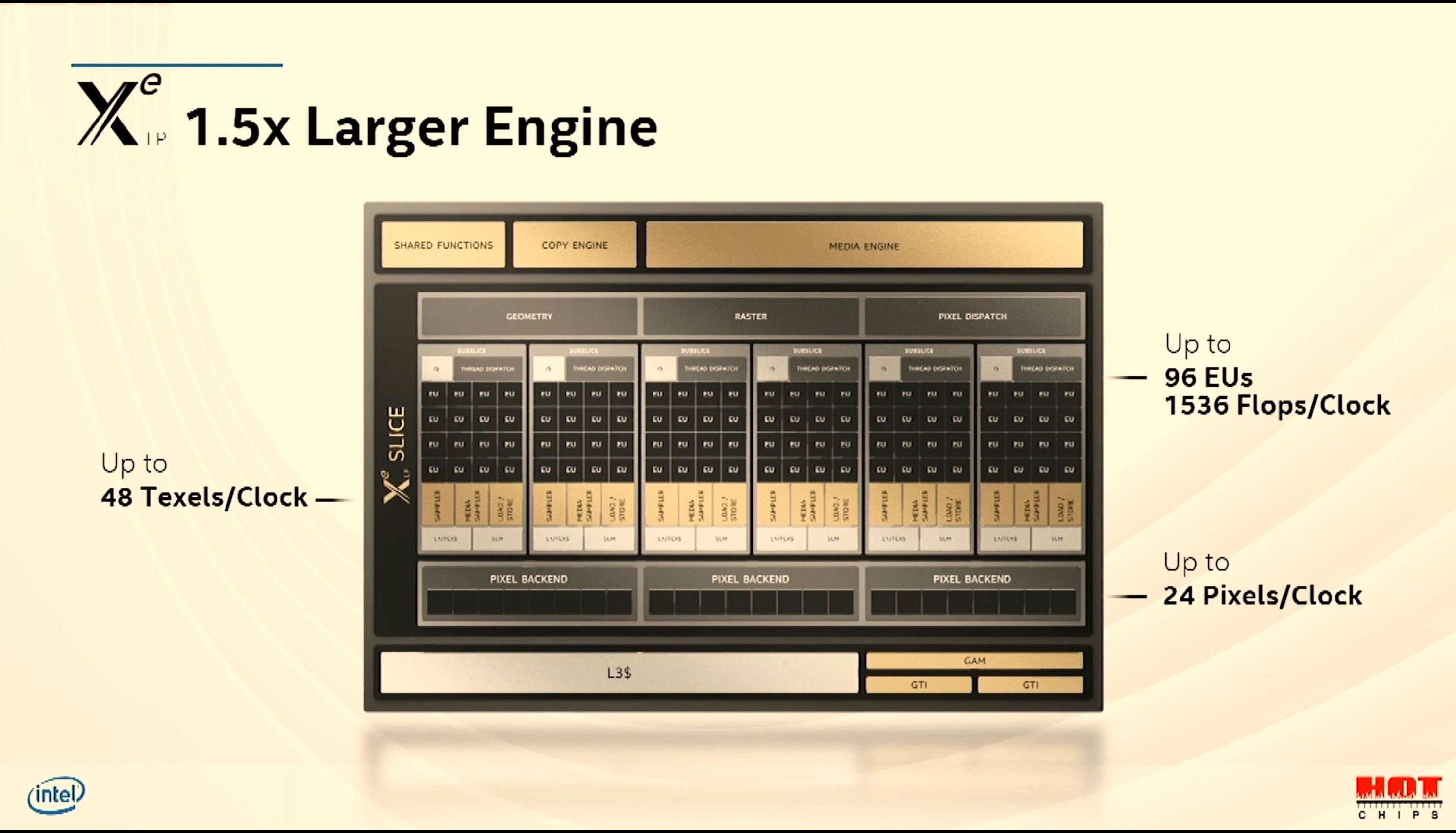
08:49PM EDT - 1.5x larger GPU EUs with scaled assets
08:49PM EDT - 96 EUs, 1536 32-bit ops/clock
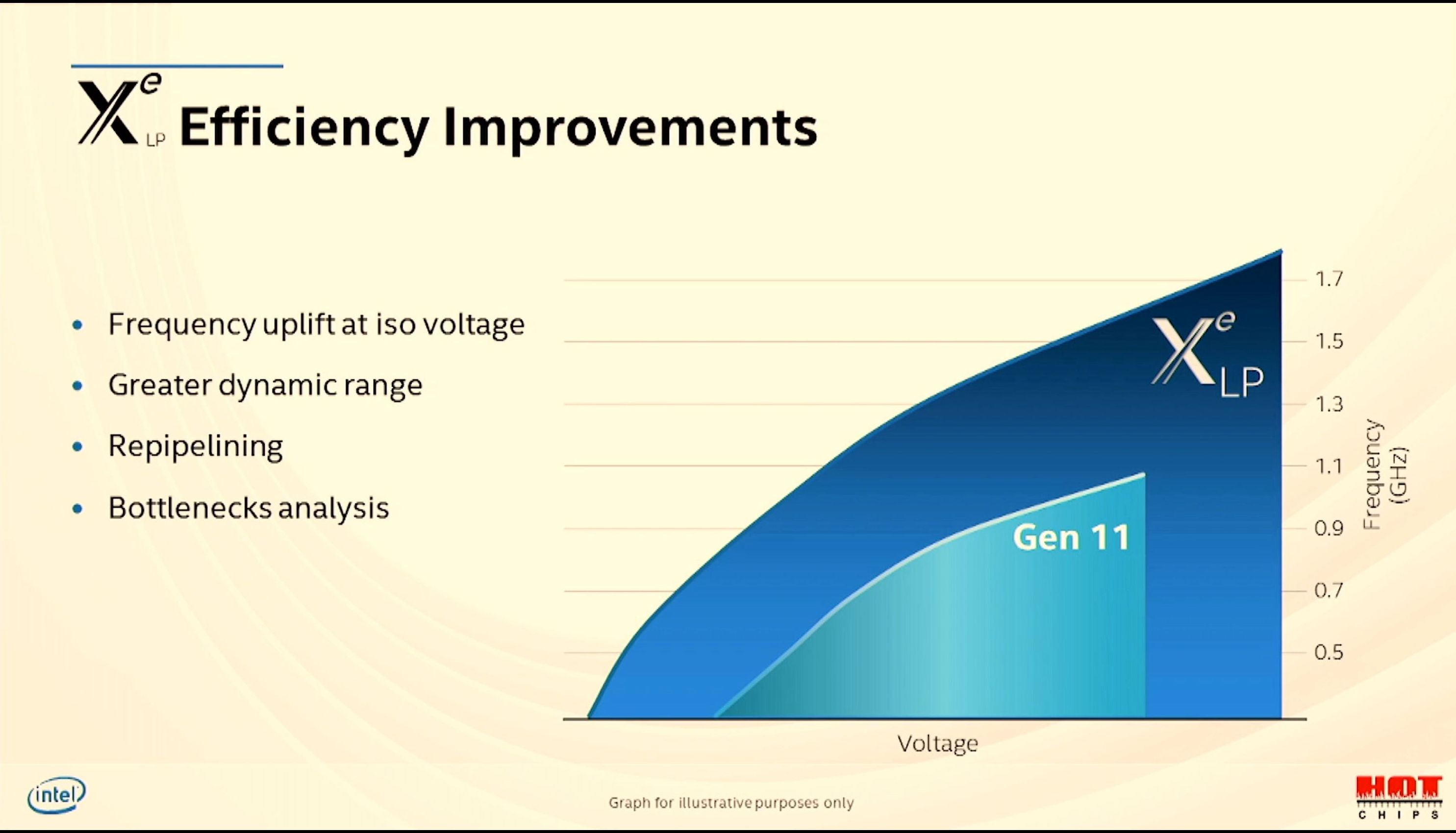
08:50PM EDT - Frequency is also 1.5x
08:51PM EDT - Tiger Lake Xe has greater dynamic range
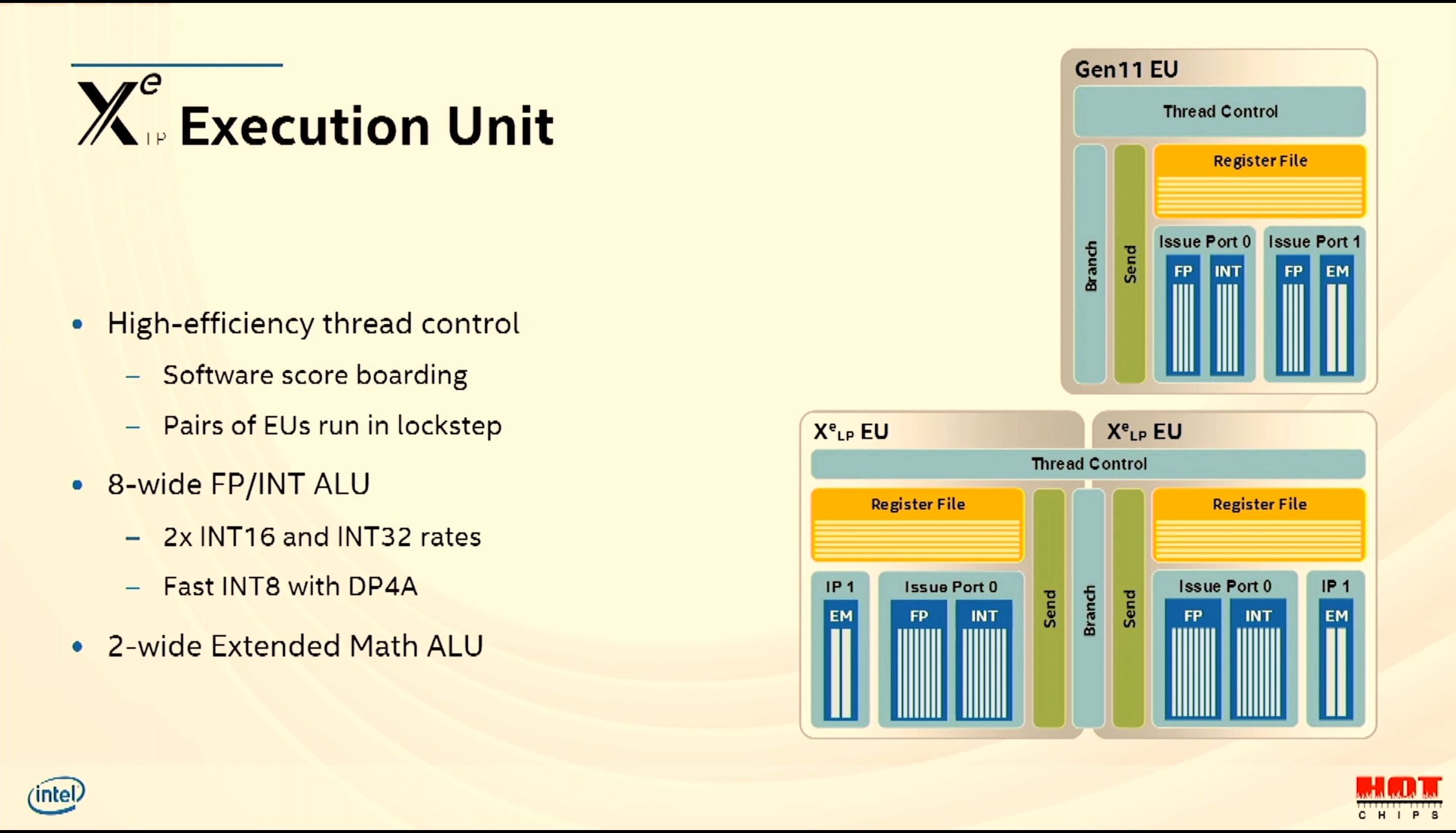
08:51PM EDT - software score boarding per EU
08:52PM EDT - Pairs of EUs run in lockstep due to shared thread control
08:52PM EDT - 2xINT16 and INT32 rates, fast INT8 dot-product that accumulates into one INT32 result
08:52PM EDT - Each subslice has one L1, and up to 16 MB L3

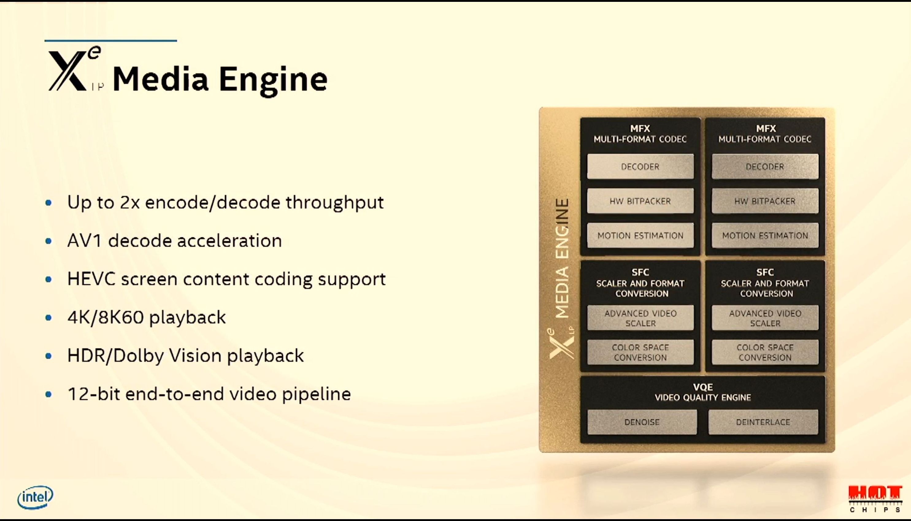
08:54PM EDT - AV1 support
08:54PM EDT - XeHP parts in the lab
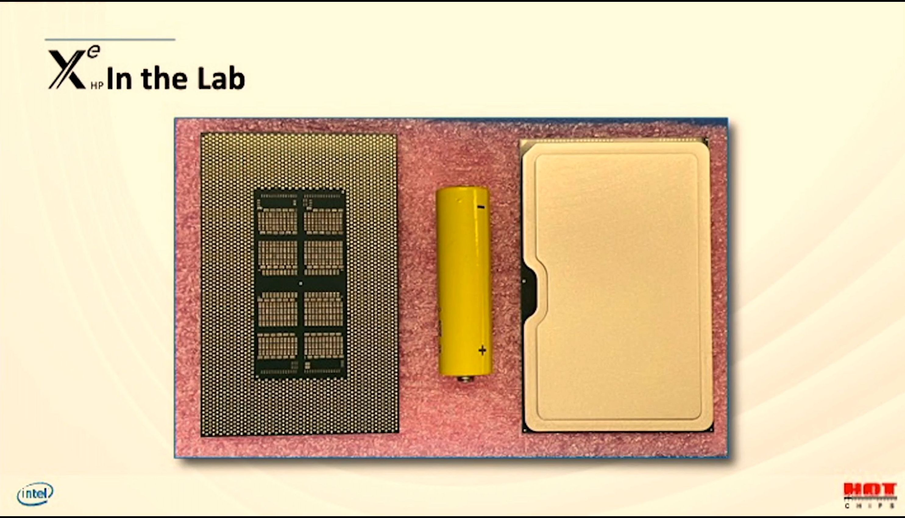
08:55PM EDT - XeHP up to 4 tiles
08:55PM EDT - 1 tile can to 10.6 GFLOP FP32
08:56PM EDT - 2 tile can to 21161 GFLOP FP32
08:56PM EDT - 4-tile can do ~42k GFLOP FP32
08:56PM EDT - Shows XeHP can scale
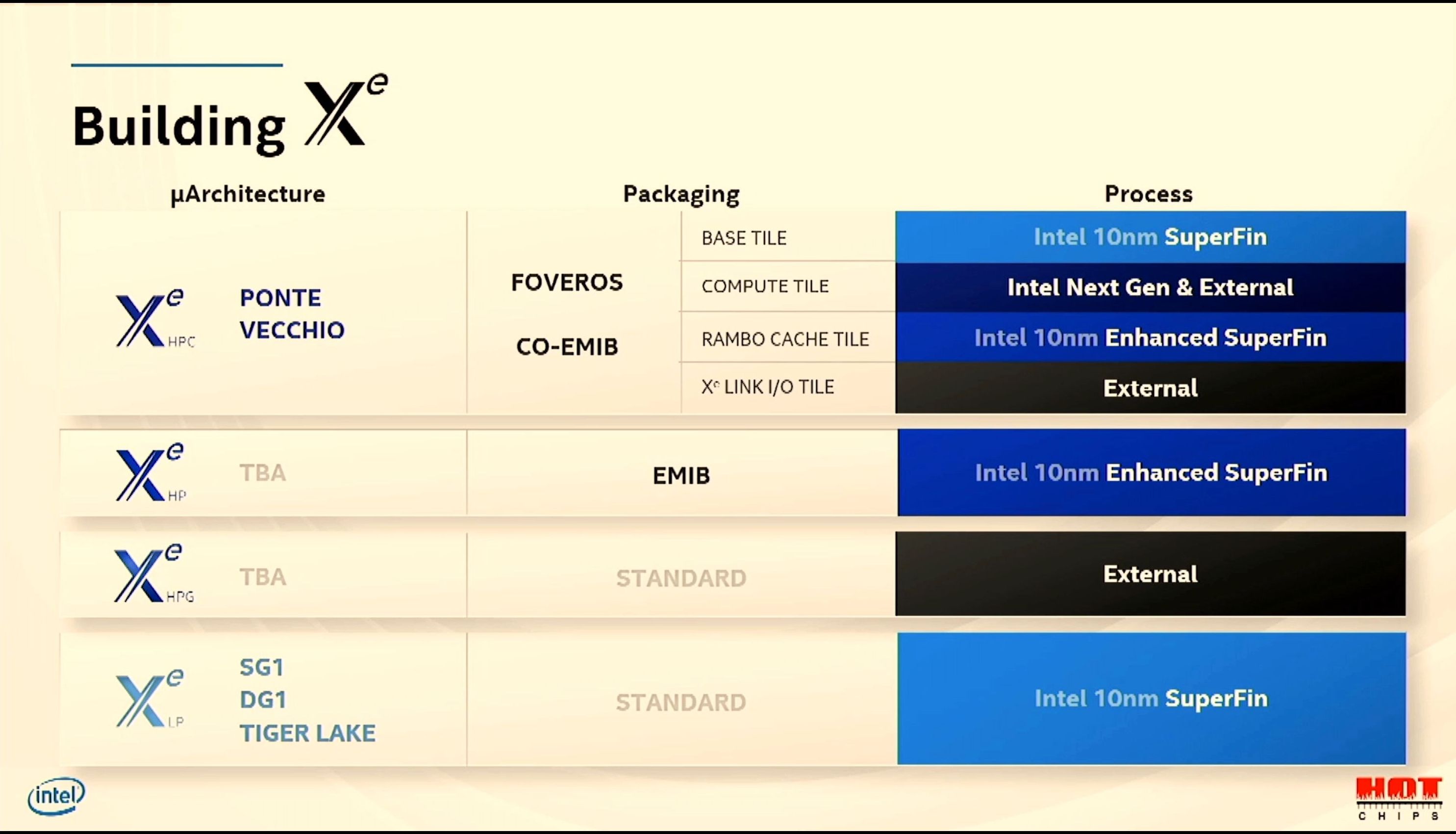
08:57PM EDT - Xe will spread across different nodes and manufacturing
08:58PM EDT - Q&A time
08:58PM EDT - Q: Xe Matrix via AMX? A: There will be an API, disclosed later
08:58PM EDT - Q: Open source driver code? A: Yes, for integrated and discrete
08:59PM EDT - Q: Why 1 RT unit per 16 EUs A: That seemed like the proper scalability. RT throughput can be modulated too - it isn't just a fixed size thing. No details at this time.
09:00PM EDT - Q: Tile-to-tile vs Xe Link ? A: Tile-to-tile is internal protocol in XeMF, but XeLink exposes the protocol, no details but lightweight
09:00PM EDT - Q: CXL? A: There's an intent to support, still working out the details
09:01PM EDT - Q: CPU to GPU comms? A: For XeHPC there is an intent to support CXL
09:02PM EDT - Q: Why are 3D fixed functions optional? A: Not all areas need 3D, like XeHPC. Can turn them off at design time if needed. GPUs can't always carry baggage in specified products
09:03PM EDT - Q: Threads in an EU? A: Not changed much. 1 or 2, in TGL supports 7, little higher in the others
09:04PM EDT - Q: API for ray tracing? A: The standard ones. Khronos, MS. For the high-end rendering, there will be OneAPI for more production type rendering. More details later, similar to embree on CPU
09:04PM EDT - That's a wrap. Next up is Xbox


28 Comments
View All Comments
Smell This - Tuesday, August 18, 2020 - link
It is not fair to Chipzilla, but graphic progress using bolt-on EUs has been a losing proposition for a long time. Xe is a simply faster, re-ordered and expanded EUs in an HD Graphics container. Xe is something like 768:96:16 --- see GT1 to GT4!
It is still 128-bit wide FPU /EU executing 8 16-bit or 4 32-bit operations per clock cycle with the re-ordered SIM blocks. It may be functional, but it is still a bolt-on (with a new double ring bus!)
mikk - Saturday, August 22, 2020 - link
Marginally better performance, did you see reviews? And also there is no 2-3x space difference, this is nonsense. You are unaware that (initial) Tigerlake and Renoir both use LPDDR4x-4266 at best which makes it super hard to scale iGPU performance up linearly, it's almost impossible. Furthermore AMDs design has fewer units but on the same time a much higher iGPU clock speed. i7-1165G7 Xe can go to up to 1.3 Ghz while Ryzen 4800U can go up to 1.75 Ghz. At 1.75 Ghz Vega 8 can do 1.79 Tflop FP32, a theroetical Xe LP 1.75 Ghz could do 2.69 Tflop, so the compute units on Tigerlake are much more powerful. Even if iGPU Vega would have more units it would struggle to hold this clocks speed in a low power environment and would struggle with the bandwidth feeding the additional units.AbRASiON - Tuesday, August 18, 2020 - link
I just want laptop with dock that can do 2x4k at a good reliable windows frame rate, playing video, moving windows around ETcJayNor - Tuesday, August 18, 2020 - link
"08:38PM EDT - Add new capabilities - matrix tensors, ray tracing, virtualization, etc"Any extra info on virtualization? What was added to support that?
JayNor - Tuesday, August 18, 2020 - link
Is the Xe memory fabric PCIE version 5.0?The XeLink description appears to be a central point for communicating with the system. Is it also being used for connection to the two per node CPUs?
JayNor - Wednesday, August 19, 2020 - link
"08:38PM EDT - Goals: increase SIMD lanes from 10s to 1000s""08:42PM EDT - 16 EUs = 128 SIMD lanes"
So, are they extending SIMD width across multiple tiles?
Yojimbo - Wednesday, August 19, 2020 - link
I assume what you call a tile and what they call a tile are two different things. There are 16 EUs per compute subslice. The number of compute subslices per compute slice is variable, but at least one of their chips has 96 EUs in a compute slice. So perhaps they are extending SIMD width across subslices within a compute slice, perhaps to the entire compute slice, which would be 768 SIMD lanes for that 96 EU compute slice. All of that happens within one tile, as what they call a tile is an element connected to other elements by their EMIB technology. Although I didn't notice it stated explicitly, perhaps one tile can be comprised of more than one compute slice.JayNor - Wednesday, August 19, 2020 - link
Not explained what single GPU implies, but perhaps this implies a simd instruction can be executed across multiple tiles."08:47PM EDT - Mutliple tiles work as separate GPUs or a single GPU"