‘Better Yield on 5nm than 7nm’: TSMC Update on Defect Rates for N5
by Dr. Ian Cutress on August 25, 2020 9:30 AM EST
One of the key metrics on how well a semiconductor process is developing is looking at its quantitative chip yield – or rather, its defect density. A manufacturing process that has fewer defects per given unit area will produce more known good silicon than one that has more defects, and the goal of any foundry process is to minimize that defect rate over time. This will give the customers better throughput when making orders, and the foundry aims to balance that with the cost of improving the manufacturing process.
The measure used for defect density is the number of defects per square centimeter. Anything below 0.5/cm2 is usually a good metric, and we’ve seen TSMC pull some really interesting numbers, such as 0.09 defects per square centimetre on its N7 process node only three quarters after high volume manufacturing started, as was announced in November at the VLSI Symposium 2019. As it stands, the defect rate of a new process node is often compared to what the defect rate was for the previous node at the same time in development. As a result, we got this graph from TSMC’s Technology Symposium this week:
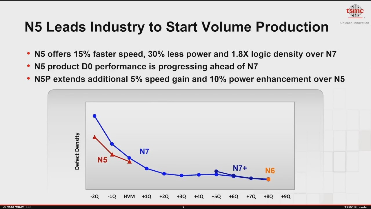
As it stands, the current N5 process from TSMC has a lower defect density than N7 did at the same time in its development cycle. TSMC. This slide from TSMC was showcased near the start of the event, and a more detailed graph was given later in the day:
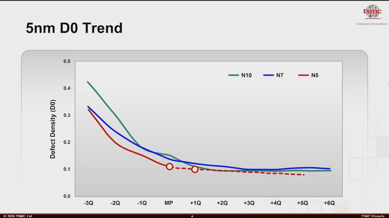
This plot is linear, rather than the logarithmic curve of the first plot. This means that TSMC’s N5 process currently sits around 0.10 to 0.11 defects per square centimeter, and the company expects to go below 0.10 as high volume manufacturing ramps into next quarter.
Part of what makes 5nm yield slightly better is perhaps down to the increasing use of Extreme UltraViolet (EUV) technology, which reduces the total number of manufacturing steps. Each step is a potential chance to decrease yield, so by replacing 4 steps of DUV for 1 step of EUV, it eliminates some of that defect rate.
TSMC’s first 5nm process, called N5, is currently in high volume production. The first products built on N5 are expected to be smartphone processors for handsets due later this year.
Related Reading
- TSMC Details 3nm Process Technology: Full Node Scaling for 2H22 Volume Production
- TSMC To Build 5nm Fab In Arizona, Set To Come Online In 2024
- TSMC & Broadcom Develop 1,700 mm2 CoWoS Interposer: 2X Larger Than Reticles
- TSMC Boosts CapEx by $1 Billion, Expects N5 Node to Be Major Success
- Early TSMC 5nm Test Chip Yields 80%, HVM Coming in H1 2020
- TSMC: 5nm on Track for Q2 2020 HVM, Will Ramp Faster Than 7nm
- TSMC: N7+ EUV Process Technology in High Volume, 6nm (N6) Coming Soon


102 Comments
View All Comments
Morawka - Wednesday, August 26, 2020 - link
Nvidia's technical prowess is really a testament to Jensen Huang leadership skills. When most companies dominate their respective markets, they get complacent. Nvidia has managed to keep innovating while dominating the competition. I wish I could say the same for Intel. Perhaps there is a cultural aspect that contributes to the high levels of innovation over at Nvidia.Spunjji - Thursday, August 27, 2020 - link
Intel have to focus on both manufacturing and chip design, which probably doesn't help with how bloated their corporate structure has become. They also came of age with an effective monopoly and extended it through anti-competitive shenanigans and marketing, so there's been no real incentive for them to be any other way - they can always bully competitors out of their core markets whenever things get dicey for them.Nvidia, on the other hand, had to compete in a much more competitive market for a longer time, and have always focused much more keenly on graphics processor design. When they've tried to diversify it hasn't been so great (Tegra), and they've had some hilarious missteps directly overseen by Huang (wood screws!), but they appear to have actually learned from that and refocused back on core competencies. Even so, they've had their own share of anti-competitive and anti-consumer practices, and I do worry that this has been worsening noticeably in the past few years.
Spunjji - Wednesday, August 26, 2020 - link
That is one weird rationalisation for a stupid decision."We could have had an even better product, but we're so awesome that we decided not to" 🤡
You're probably right about their architecture. We'll see what Ampere brings, but unless it fails to move the bar much from Turing, it should keep them well in the lead at the high-end.
vladx - Wednesday, August 26, 2020 - link
"That is one weird rationalisation for a stupid decision."It's stupid in your view as a customer, meanwhile as a company would rather have higher profits than unnecessary gains at this time.
Spunjji - Thursday, August 27, 2020 - link
Honestly, I'd accept that response if I could see figures to back it up, but we don't have access to them. Speaking theoretically, I'd be very surprised if manufacturing such massive power-hungry chips on a less-dense process weren't costing them significantly in terms of yields. It's already clear they've blown the power budget too, but for some reason nobody cares about that? All in all, I'm getting big Fermi vibes from this generation.Whether or not AMD are able to repeat the feat ATi managed back then of introducing a more power-efficient and cost-effective design to counter Nvidia's juggernaut remains to be seen, though. I have hope but anticipate disappointment.
vladx - Friday, August 28, 2020 - link
Must really suck being an AMD fanboi always expecting to be disappointed.Kishoreshack - Tuesday, August 25, 2020 - link
Unfortunately no 5nm cpu or GPU launches for another year & a halfVitor - Wednesday, August 26, 2020 - link
Unless you are Apple.Anymoore - Wednesday, August 26, 2020 - link
It's doubtful fewer masks improved yield, it didn't do anything for N7+ or N6.Wilco1 - Wednesday, August 26, 2020 - link
Both N7+ and N6 are the lowest in the graphs. So all EUV processes, including N5, show a much faster yield improvement than N7.