Apple Announces The Apple Silicon M1: Ditching x86 - What to Expect, Based on A14
by Andrei Frumusanu on November 10, 2020 3:00 PM EST- Posted in
- Apple
- Apple A14
- Apple Silicon
- Apple M1
Today, Apple has unveiled their brand-new MacBook line-up. This isn’t an ordinary release – if anything, the move that Apple is making today is something that hasn’t happened in 15 years: The start of a CPU architecture transition across their whole consumer Mac line-up.
Thanks to the company’s vertical integration across hardware and software, this is a monumental change that nobody but Apple can so swiftly usher in. The last time Apple ventured into such an undertaking in 2006, the company had ditched IBM’s PowerPC ISA and processors in favor of Intel x86 designs. Today, Intel is being ditched in favor of the company’s own in-house processors and CPU microarchitectures, built upon the Arm ISA.
The new processor is called the Apple M1, the company’s first SoC designed with Macs in mind. With four large performance cores, four efficiency cores, and an 8-GPU core GPU, it features 16 billion transistors on a 5nm process node. Apple’s is starting a new SoC naming scheme for this new family of processors, but at least on paper it looks a lot like an A14X.
Today’s event contained a ton of new official announcements, but also was lacking (in typical Apple fashion) in detail. Today, we’re going to be dissecting the new Apple M1 news, as well as doing a microarchitectural deep dive based on the already-released Apple A14 SoC.
The Apple M1 SoC: An A14X for Macs
The new Apple M1 is really the start of a new major journey for Apple. During Apple’s presentation the company didn’t really divulge much in the way of details for the design, however there was one slide that told us a lot about the chip’s packaging and architecture:
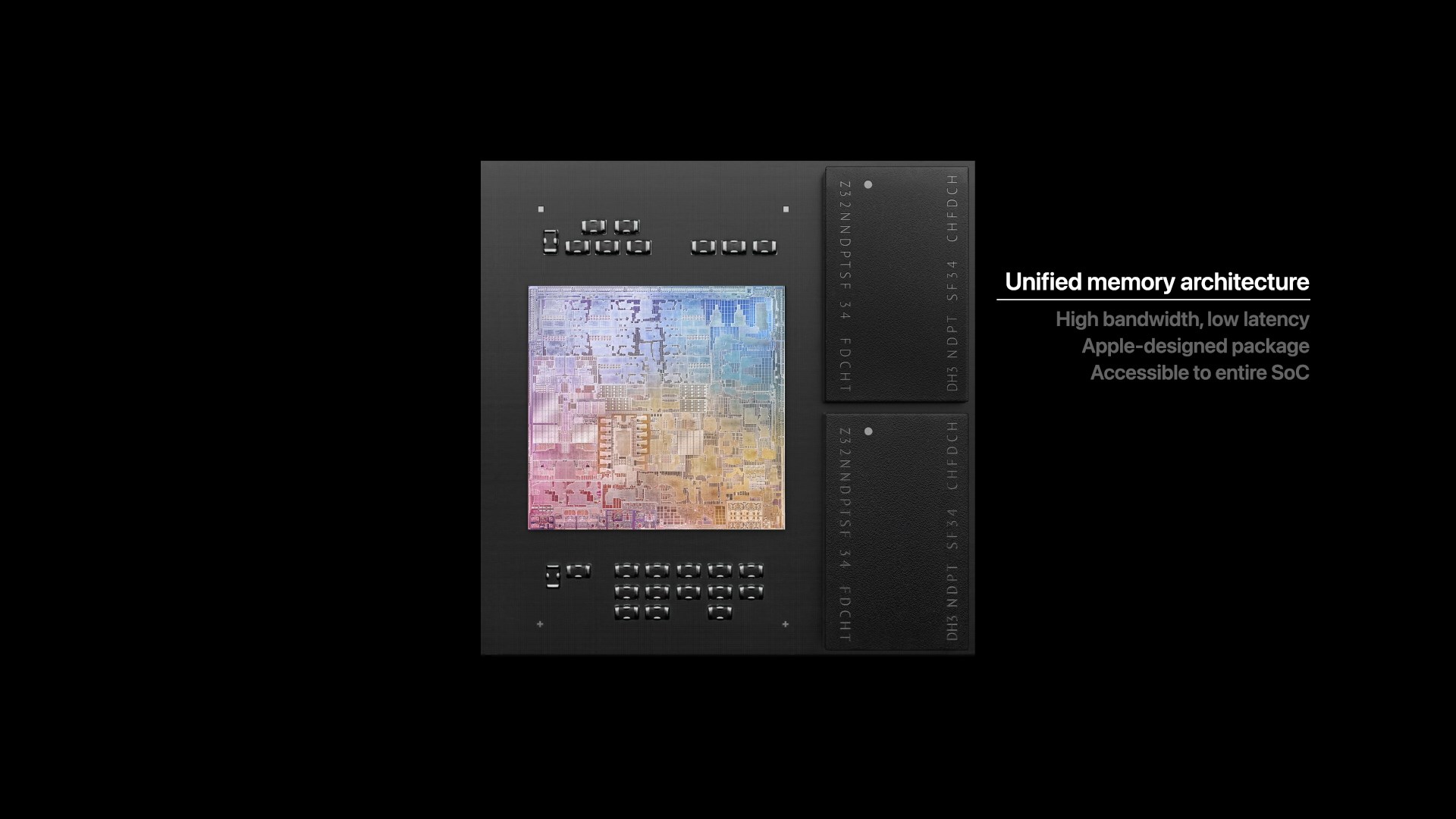
This packaging style with DRAM embedded within the organic packaging isn't new for Apple; they've been using it since the A12. However it's something that's only sparingly used. When it comes to higher-end chips, Apple likes to use this kind of packaging instead of your usual smartphone POP (package on package) because these chips are designed with higher TDPs in mind. So keeping the DRAM off to the side of the compute die rather than on top of it helps to ensure that these chips can still be efficiently cooled.
What this also means is that we’re almost certainly looking at a 128-bit DRAM bus on the new chip, much like that of previous generation A-X chips.
On the very same slide, Apple also seems to have used an actual die shot of the new M1 chip. It perfectly matches Apple’s described characteristics of the chip, and it looks looks like a real photograph of the die. Cue what's probably the quickest die annotation I’ve ever made:
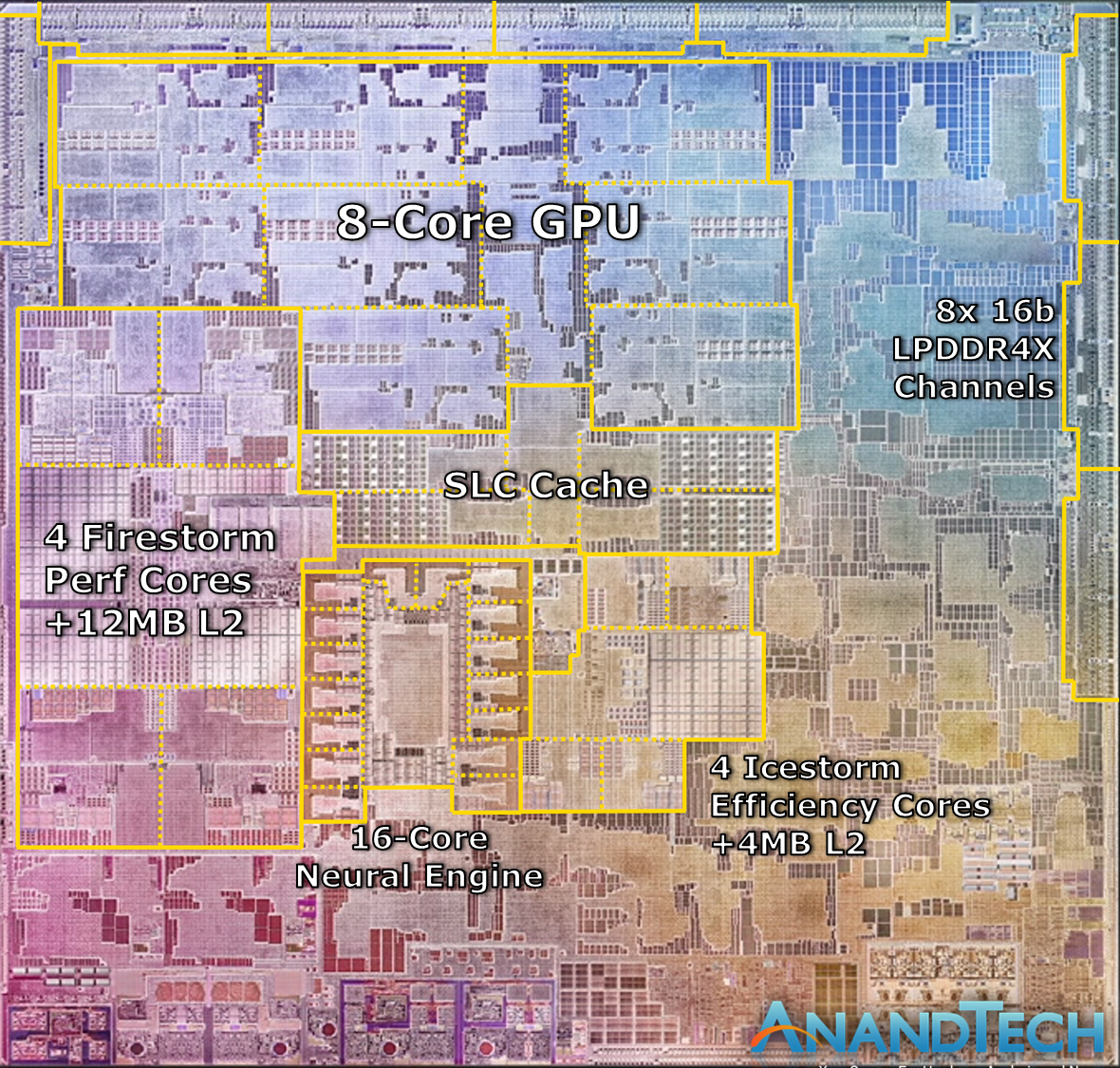
We can see the M1’s four Firestorm high-performance CPU cores on the left side. Notice the large amount of cache – the 12MB cache was one of the surprise reveals of the event, as the A14 still only featured 8MB of L2 cache. The new cache here looks to be portioned into 3 larger blocks, which makes sense given Apple’s transition from 8MB to 12MB for this new configuration, it is after all now being used by 4 cores instead of 2.
Meanwhile the 4 Icestorm efficiency cores are found near the center of the SoC, above which we find the SoC’s system level cache, which is shared across all IP blocks.
Finally, the 8-core GPU takes up a significant amount of die space and is found in the upper part of this die shot.
What’s most interesting about the M1 here is how it compares to other CPU designs by Intel and AMD. All the aforementioned blocks still only cover up part of the whole die, with a significant amount of auxiliary IP. Apple made mention that the M1 is a true SoC, including the functionality of what previously was several discrete chips inside of Mac laptops, such as I/O controllers and Apple's SSD and security controllers.
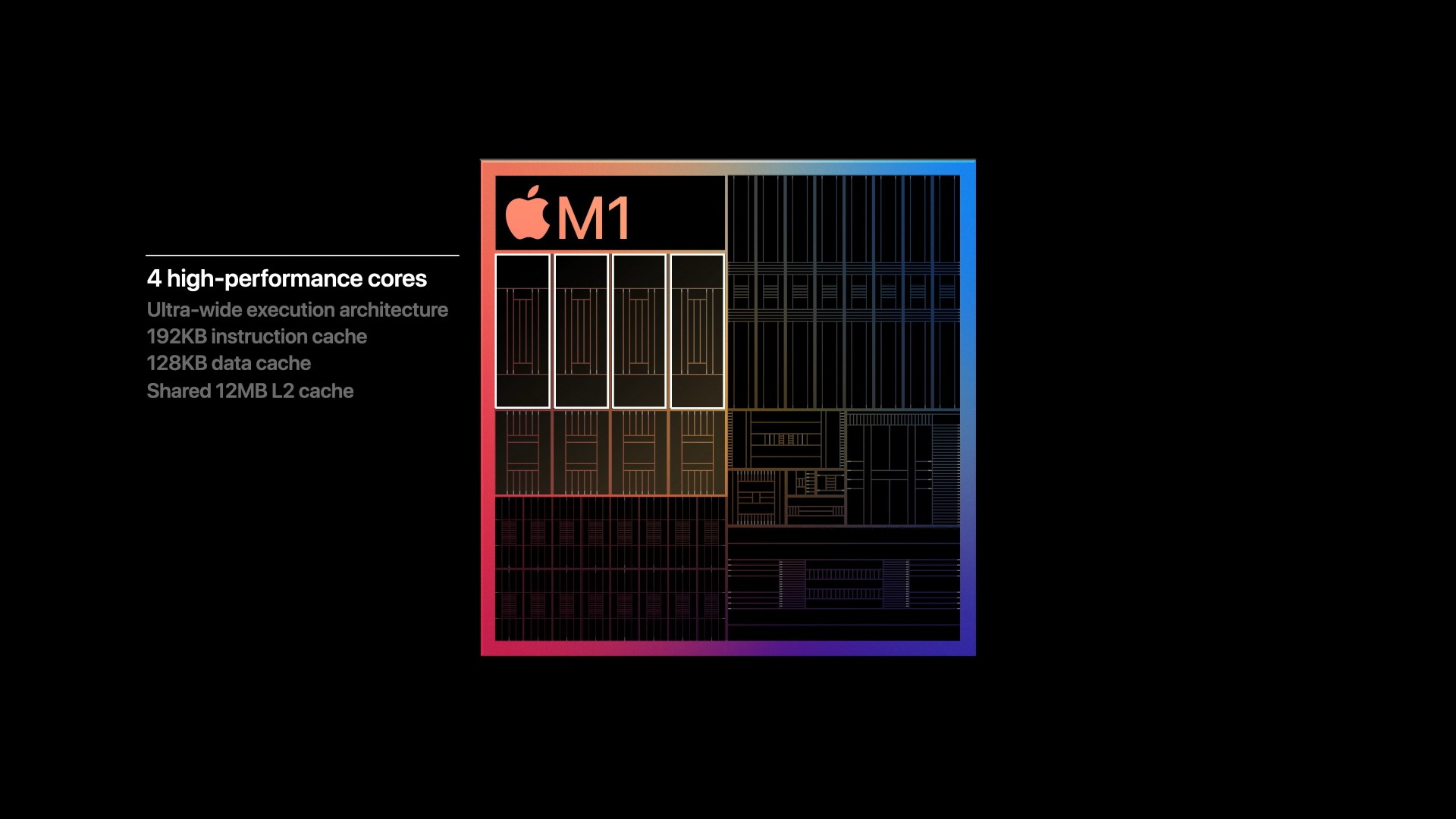
The new CPU core is what Apple claims to be the world’s fastest. This is going to be a centre-point of today’s article as we dive deeper into the microarchitecture of the Firestorm cores, as well look at the performance figures of the very similar Apple A14 SoC.
With its additional cache, we expect the Firestorm cores used in the M1 to be even faster than what we’re going to be dissecting today with the A14, so Apple’s claim of having the fastest CPU core in the world seems extremely plausible.

The whole SoC features a massive 16 billion transistors, which is 35% more than the A14 inside of the newest iPhones. If Apple was able to keep the transistor density between the two chips similar, we should expect a die size of around 120mm². This would be considerably smaller than past generation of Intel chips inside of Apple's MacBooks.
Road To Arm: Second Verse, Same As The First
Section by Ryan Smith
The fact that Apple can even pull off a major architectural transition so seamlessly is a small miracle, and one that Apple has quite a bit of experience in accomplishing. After all, this is not Apple’s first-time switching CPU architectures for their Mac computers.
The long-time PowerPC company came to a crossroads around the middle of the 2000s when the Apple-IBM-Motorola (AIM) alliance, responsible for PowerPC development, increasingly struggled with further chip development. IBM’s PowerPC 970 (G5) chip put up respectable performance numbers in desktops, but its power consumption was significant. This left the chip non-viable for use in the growing laptop segment, where Apple was still using Motorola’s PowerPC 7400 series (G4) chips, which did have better power consumption, but not the performance needed to rival what Intel would eventually achieve with its Core series of processors.
And thus, Apple played a card that they held in reserve: Project Marklar. Leveraging the flexibility of the Mac OS X and its underlying Darwin kernel, which like other Unixes is designed to be portable, Apple had been maintaining an x86 version of Mac OS X. Though largely considered to initially have been an exercise in good coding practices – making sure Apple was writing OS code that wasn’t unnecessarily bound to PowerPC and its big-endian memory model – Marklar became Apple’s exit strategy from a stagnating PowerPC ecosystem. The company would switch to x86 processors – specifically, Intel’s x86 processors – upending its software ecosystem, but also opening the door to much better performance and new customer opportunities.
The switch to x86 was by all metrics a big win for Apple. Intel’s processors delivered better performance-per-watt than the PowerPC processors that Apple left behind, and especially once Intel launched the Core 2 (Conroe) series of processors in late 2006, Intel firmly established itself as the dominant force for PC processors. This ultimately setup Apple’s trajectory over the coming years, allowing them to become a laptop-focused company with proto-ultrabooks (MacBook Air) and their incredibly popular MacBook Pros. Similarly, x86 brought with it Windows compatibility, introducing the ability to directly boot Windows, or alternatively run it in a very low overhead virtual machine.
The cost of this transition, however, came on the software side of matters. Developers would need to start using Apple’s newest toolchains to produce universal binaries that could work on PPC and x86 Macs – and not all of Apple’s previous APIs would make the jump to x86. Developers of course made the jump, but it was a transition without a true precedent.
Bridging the gap, at least for a bit, was Rosetta, Apple’s PowerPC translation layer for x86. Rosetta would allow most PPC Mac OS X applications to run on the x86 Macs, and though performance was a bit hit-and-miss (PPC on x86 isn’t the easiest thing), the higher performance of the Intel CPUs helped to carry things for most non-intensive applications. Ultimately Rosetta was a band-aid for Apple, and one Apple ripped off relatively quickly; Apple already dropped Rosetta by the time of Mac OS X 10.7 (Lion) in 2011. So even with Rosetta, Apple made it clear to developers that they expected them to update their applications for x86 if they wanted to keeping selling them and to keep users happy.
Ultimately, the PowerPC to x86 transitions set the tone for the modern, agile Apple. Since then, Apple has created a whole development philosophy around going fast and changing things as they see fit, with only limited regard to backwards compatibility. This has given users and developers few options but to enjoy the ride and keep up with Apple’s development trends. But it has also given Apple the ability to introduce new technologies early, and if necessary, break old applications so that new features aren’t held back by backwards compatibility woes.
All of this has happened before, and it will all happen again starting next week, when Apple launches their first Apple M1-based Macs. Universal binaries are back, Rosetta is back, and Apple’s push to developers to get their applications up and running on Arm is in full force. The PPC to x86 transition created the template for Apple for an ISA change, and following that successful transition, they are going to do it all over again over the next few years as Apple becomes their own chip supplier.
A Microarchitectural Deep Dive & Benchmarks
In the following page we’ll be investigating the A14’s Firestorm cores which will be used in the M1 as well, and also do some extensive benchmarking on the iPhone chip, setting the stage as the minimum of what to expect from the M1:


644 Comments
View All Comments
grayson_carr - Wednesday, November 11, 2020 - link
There are about 260 million x86 computers sold per year, and the latest estimates say 62.5% (162 million) of those contain Intel chips. Apple sells around 20 million Macs per year, so Apple buys over 12% of all Intel x86 chips. If that's not a major customer, then I don't know what is. The only companies that sell more computers than Apple are Lenovo, HP, and Dell.GC2:CS - Tuesday, November 10, 2020 - link
Have you tried to run spec in low power mode to see how the power efficiency changes ?Or at least the clock speed table. It is 1,85 Ghz down from 2,66 for Lightning.
If the small cores are significally more powerfull now, how do they compare to A55 (sigh) ?
Which Big core would be in some way equivalent to this year and previous year small cores ?
Can we say something like A10 zephyr was like A4 mainCPU and Icestorm is like a cyclone core now ?
Andrei Frumusanu - Tuesday, November 10, 2020 - link
I'll follow up on LPM figures, but it's running at 1294MHz which is kinda slow.~4x faster than an A55, ~ same power, ~2x better energy efficiency: https://www.anandtech.com/show/14072/the-samsung-g...
The new small cores are roughly in line with an A9 big core.
I don't have data pre-A9.
Fritzkier - Tuesday, November 10, 2020 - link
I still don't understand why ARM doesn't make new efficiency cores...eastcoast_pete - Tuesday, November 10, 2020 - link
I guess ARM is too busy chasing after "big game", servers etc. Good efficiency cores aren't sexy enough for Aging Risc Machines, I guess. Let's hope archs like RISC-V catch on and up, and bust the ARM monopoly in mobile.Spunjji - Thursday, November 12, 2020 - link
My best guess: they have limited resources, and they don't *have* to improve on A55. Most of their customers don't really seem to care.Spunjji - Thursday, November 12, 2020 - link
Damn! Thanks for the additional context, Andrei.name99 - Tuesday, November 10, 2020 - link
You can ballpark a lot of it. If you're willing to live on the sane side of reality, for most purposes, and within a sane range of interpolation:- IPC is pretty constant across frequency (so performance scales as f^1)
- total energy use scales like f^2
- power scales like f^3
name99 - Friday, November 13, 2020 - link
Follow up to the above. If we assume the multiplier is 6%, which seems to be what all the data indicates (3 vs 3.2GHz), then f^3 gives us that the additional power of an M1 big core at full speed is ~1.2x the A14 big core, so 6W rather than 5.So worst case CPU scenario would be maybe 24W (sure, also the small cores, but they're going to be miniscule). Throw in worst case GPU is maybe, what, 8W?
This suggests that
- in theory an MBA might have to throttle. What can that chassis dissipate comfortably? 15W? So you might have to dial the cores down to 2.5GHz or so. But not a huge deal.
- and that MBP and mac mini are both going to be way overspecced in their fans, unless you plan to run them in hot poorly ventilated closets.
- perhaps if you're planning to play some seriously well threaded games you may notice the MBA vs MBP/mini difference, but not otherwise.
Can anyone see a fault in my reasoning? Or to put it differently, do people find that playing the most aggressive games on iPad Pro ever throttles? I'd guess the iPad Pro has about the same thermal dissipation as an MBA.
HurleyBird - Tuesday, November 10, 2020 - link
"We don’t know if this is comparing M1 to an AMD Renoir chip or an Intel ICL or TGL chip"You're being extremely generous. This is Apple we're talking about so that kind of comparison would be a nice surprise, but we're probably dealing with a low-end Comet Lake, assuming this graph is actually based on any kind of real data and isn't just a wishful guesstimation.
For context, on the new MDP page the claim "up to 2.8x faster processing performance than the previous generation," the footnote lists a 1.4GHZ quad core processor. This would presumably be the i5-8257U in the previous gen MBP.
In Apple speak, "up to" means "we cherry picked the absolute best benchmark." I'm sure you can find benchmarks where , say, a 4800U is around that 2.8x speedup compared to the i5-8257U. I found a benchmark (CB R15 Multi) that is around 2.43x almost immediately.
So, that's Renoir out of the question. It's too close to M1 performance to ever work in that graph. ICL/TGL might be possible in an MT workload, but I wouldn't put money on it.
I'll note that if M1 is faster than Renoir, which is certainly possible, it's likely slower than Cezanne.