Jim Keller Becomes CTO at Tenstorrent: "The Most Promising Architecture Out There"
by Dr. Ian Cutress on January 5, 2021 9:50 PM EST- Posted in
- CPUs
- SoCs
- AI
- Jim Keller
- ML
- Tenstorrent
- Greyskull
- Wormhole

It is high praise when someone like Jim Keller says that your company ‘has made impressive progress, and has the most promising architecture out there’. That praise means twice as much if Keller actually joins the company. Today Tenstorrent is announcing that Jim Keller, compute architect extraordinaire, has joined the company as its Chief Technology Officer, President, and joins the company board.
To our regular audience, Jim Keller is a known expert in all things computer architecture. His history starts at DEC, designing Alpha processors, before moving to a first stint at AMD for two years working to launch K7 and K8. Keller spent four years as Chief Architect at SiByte/Broadcom designing MIPS for network interfaces, four years at P.A. Semi, four years at Apple (A4+A5), then back to AMD for three years two years as Corporate VP and Chief Cores Architect in charge of the new generation of CPU architectures, K12 and Zen. This was then followed with two years at Tesla as VP of Autopilot Hardware Engineering creating the Full Self-Driving chip, then two years as Intel’s Senior VP of the Silicon Engineering Group, before leaving in June 2020. Since his departure from Intel, a number of key industry analysts (and ourselves) have been guessing where Jim would land. He briefly appeared in the audience of Elon Musk’s Neuralink presentation in August 2020, alongside Lex Fridman.
| Jim Keller: Work Experience | ||||
| AnandTech | Company | Title | Important Product |
|
| 1980s | 1998 | DEC | Architect | Alpha |
| 1998 | 1999 | AMD | Lead Architect | K7, K8 |
| 1999 | 2000 | SiByte | Chief Architect | MIPS Networking |
| 2000 | 2004 | Broadcom | Chief Architect | MIPS Networking |
| 2004 | 2008 | P.A. Semi | VP Engineering | Low Power Mobile |
| 2008 | 2012 | Apple | VP Engineering | A4 / A5 Mobile |
| 8/2012 | 9/2015 | AMD | Corp VP and Chief Cores Architect |
Skybridge / K12 (+ Zen) |
| 1/2016 | 4/2018 | Tesla | VP Autopilot Hardware Engineering |
Fully Self-Driving (FSD) Chip |
| 4/2018 | 6/2020 | Intel | Senior VP Silicon Engineering |
? |
| 2021 | Tenstorrent | President and CTO | TBD | |
Today Tenstorrent reached out to inform us that Jim Keller has taken the position of President and Chief Technology Officer of the company, as well as being a member of its Board of Directors. Jim's role, based on his previous expertise, would appear to be in the design of future products for the company as well as building on the team at Tenstorrent to succeed in that goal.
![]()
CEO Ljubisa Bajic confirmed Jim’s appointment as President and CTO of the company, stating that:
Tenstorrent was founded on the belief that the ongoing shift towards ML-centric software necessitates a corresponding transformation in computational capabilities. There is nobody more capable of executing this vision than Jim Keller, a leader who is equally great at designing computers, cultures, and organizations. I am thrilled to be working with Jim and beyond excited about the possibilities our partnership unlocks.
Tenstorrent is a pure-play fab-less AI chip design and software company, which means that they create and design silicon for machine learning, then use a foundry to make the hardware, then work with partners to create solutions (as in, chips + system + software + optimizations for that customer). For those that know this space, this makes the company sound like any of the other 50 companies out in the market that seem to be doing the same thing. The typical split with pure-play fabless AI chip design companies is whether they are focused on training or inference: Tenstorrent does both, and is already in the process of finalizing its third generation processor.
Founded in 2016, Tenstorrent has around 70 employees between Toronto and Austin. The critical members of the company all have backgrounds in silicon design: the CEO led power and performance architecture at AMD as well as system architecture for Tegra at NVIDIA, the head of system software spent 16 years across AMD and Altera, and there’s expertise from neural network accelerator design from Intel, GPU systems engineering at AMD, Arm CPU verification leads, IO virtualization expertise at AMD, Intel’s former neural network compiler team lead, as well as AMD’s former security and network development lead. It sounds like Jim will fit right in, as well as have a few former colleagues working alongside him.
Tenstorrent’s current generation product is Grayskull, a ~620mm2 processor built on GF’s 12nm that was initially designed as an inference accelerator and host. It contains 120 custom cores in a 2D bidirectional mesh, and offers 368 TeraOPs of 8-bit compute for only 65 W. Each of the 120 custom cores has a packet management engine for data control, a packet compute engine that contains Tenstorrent’s custom TENSIX cores, and five RISC cores for non-standard operations, such as conditionals. The chip focuses on sparse tensor operations by optimizing matrix operations into compressed packets, enabling pipeline parallelization of the compute steps both through the graph compiler and the packet manager. This also enables dynamic graph execution, and compared to some other AI chip models, allows both compute and data transfer asynchronously, rather than specific compute/transfer time domains.
Grayskull is currently shipping to Tenstorrent’s customers, all of which are still undisclosed.
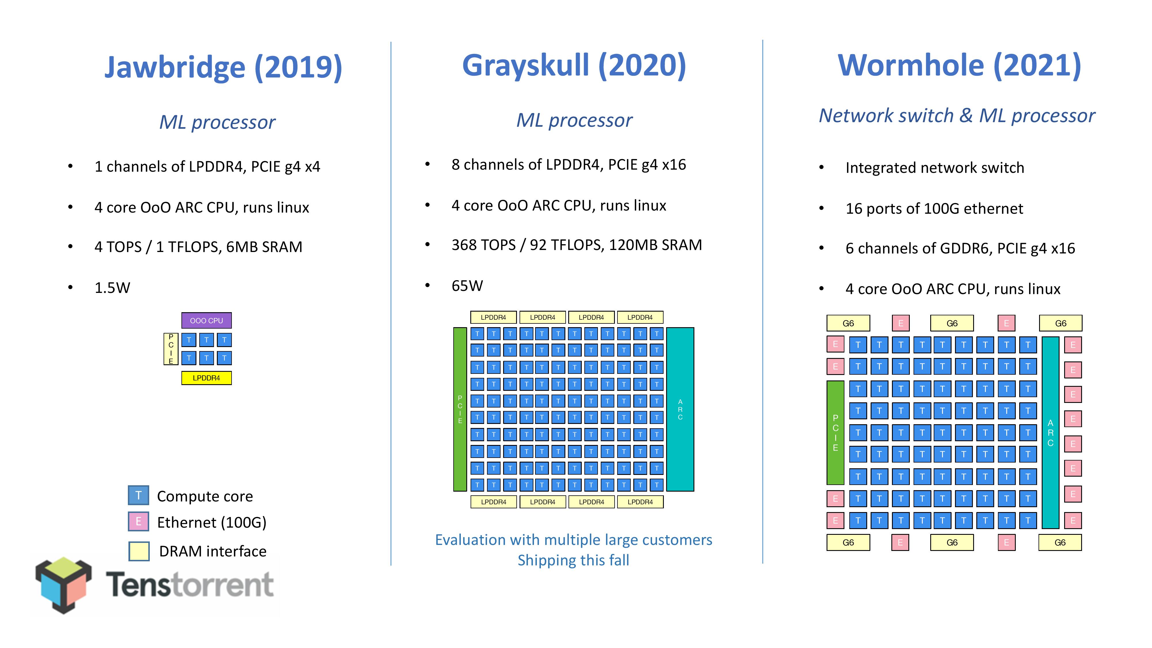
The next generation chip, known as Wormhole, is more focused on training than acceleration, and also bundles in a 16x100G Ethernet port switch. The move from training to acceleration necessitates a faster memory interface, and so there are six channels of GDDR6, rather than 8 channels of LPDDR4. This might seem low compared to other AI chips discussing HBM integration, however Tenstorrent’s plan here seems to be more aligned for more mid-range cost structure, but also offering machine learning compute at a better rate of efficiency than those chips pushing the bleeding edge of frequency and process node (part of this will be in yields as well).
So where exactly does Keller fit in if the current generation is already selling, and the next generation is almost ready to go? In speaking to the CEO, I confirmed that Keller ‘will be building new and interesting stuff with us’. This seems to suggest that the vision with Keller’s involvement is going to be on 2022/2023 hardware in mind, following Tenstorrent’s overriding Software 2.0 strategy that the hardware, compiler, and run-time offer a full-stack approach to sparse (and dense) AI matrix calculations. In Jim’s own words:
Software 2.0 is the largest opportunity for computing innovation in a long time. Victory requires a comprehensive re-thinking of compute and low level software. Tenstorrent has made impressive progress, and with the most promising architecture out there, we are poised to become a next gen computing giant.
Jim Keller officially started last Wednesday, and the official wire announcement is set for 1/6, but we've been allowed to share in advance. Our request for an interview with Jim has been noted and filed, potentially for a few months down the line as the company has some more details on its platform and roadmap (I’ve also asked for an up-to-date headshot of Jim!). For those interested, I interviewed Jim back in July 2018, just after he started at Intel – you can read that interview here.
Related Reading
- Hot Chips 32 (2020) Schedule Announced: Tenstorrent
- Jim Keller Resigns from Intel, Effective Immediately
- An AnandTech Exclusive: The Jim Keller Interview
- CPU Design Guru Jim Keller Joins Intel; Completes CPU Grand Tour
- Jim Keller Leaves AMD
- AMD Announces Project SkyBridge: Pin-Compatible ARM and x86 SoCs in 2015, Android Support
- Apple A4/A5 Designer & K8 Lead Architect, Jim Keller, Returns to AMD


66 Comments
View All Comments
FullmetalBlackWolf - Friday, January 8, 2021 - link
Do you mean to say:"It is high praise when someone like Jim Keller says that your company ‘has made impressive progress, and has the most promising architecture out there’. That praise means twice as much since Keller didn't join the company."
Since the company made impressive progress which is stated by Keller, how could the praise justify by keller not joining the company? How could the praise becomes twice by him not joining the company? Shouldn't he give the company a helping hand to improve the architecture? Correct me if i am wrong. Did i misunderstood?
WaltC - Wednesday, January 6, 2021 - link
Just what we need--another Rambus! Keller's got a cushy new job...what do people *expect* him to say about the company shelling out the dough?...;) Will he last longer than two years here, I wonder?...IIRC, he wasn't able to accomplish much at Intel, although he took the job, and the pay, they offered. Talk is always cheap--show me the products and processors.alumine - Wednesday, January 6, 2021 - link
I think he ruffled too many feathers there (either management but more likely board members / investors) and didn't really get a chance to do much.You've completely dismissed his previous achievements though - DEC, AMD, Tesla, and Apple.
FunBunny2 - Friday, January 8, 2021 - link
"I think he ruffled too many feathers there "it wasn't all that many years ago that Intel, and it's zealots, based their notions of superiority on Intel's prowess at fab. those days are gone forever, so what's left? architecture? X86 is 50 years old, Itanium didn't do anything, and i960 not much. really, how much different is today's cpu core functionality different from ENIAC?
Yojimbo - Wednesday, January 6, 2021 - link
All of these designs are putting large pools of SRAM on the dies. SRAM densities are not expected to scale much over the next couple of process shrinks at TSMC, however. If a 256 Mbit SRAM cell is 5.4 mm^2 on the 5nm node and they triple their SRAM when going from 12nm to 5nm so they have 360 MB, that's over 60 mm^2 of die area spent on the SRAM.But that's for an inference chip. The Graphcore design, a training and inference chip like Tenstorrent want to create, already has 900 MB of SRAM on their 7 nm chip. If others are similar and they just scale the architecture up that might mean about 1300 MB on a 5 nm chip, which is over 200 mm^2 of die area for the SRAM pool. That's a sizable chunk of a 650 mm^2 chip. I don't know if it would work that way but it's something which has crossed my mind as these companies are putting bigger and bigger SRAM pools on these chips. Maybe the resulting power savings are worth it, but it seems like they'll be getting diminishing returns on the strategy as the process shrinks. Maybe they can get more efficient usage of the cache capacity as they refine their designs.
name99 - Wednesday, January 6, 2021 - link
"SRAM densities are not expected to scale much over the next couple of process shrinks at TSMC"This seems a very strong statement built upon extraordinarily flimsy evidence (basically taking a single data point and insisting it represents the future).
Look at the graph in this article, which suggests a much more balanced future:
https://semiwiki.com/eda/synopsys/294205-what-migh...
There are a few years for which SRAM density grows less rapidly than logic (but still grows) then a big jump once we move to CFETs.
Another direction from which it's unclear this is a catastrophe is MRAM. If MRAM scaling continues then at some point it make make sense to move many of the large pools of slowish SRAM (ie your L3/system level caches) to MRAM. As far as I can tell the jury remains out on whether such a crossover point is in our near future.
Yojimbo - Wednesday, January 6, 2021 - link
What? TSMC has said so themself. Why don't you ask me for evidence first before declaring there is "very flimsy evidence?" Strange.https://i1.wp.com/semianalysis.com/wp-content/uplo...
https://www.anandtech.com/show/16024/tsmc-details-...
So:
7 -> 5: 1.8 times logic density, 1.35 times SRAM density
5 -> 3: 1.7 times logic density, 1.25 times SRAM density.
Now, maybe their modified processes for high powered chips will have better SRAM scaling than their low power processes, but I wouldn't count on it. SRAM is also a large percentage of SoCs.
And, CFET? I am talking about real products based on a real product roadmap for the next 5 years. Not on "what might the 1 nm node look like?" starting in 2028-2030, at the earliest. Notice the word "might" and the years 2028-2030.
And then you introduce some other unproven technology, MRAM, something else that "might" make a difference.
It's sort of ironic that you accuse me of making "very strong statements" on "extraordinarily flimsy evidence" and then start talking about CFET and MRAM. And nothing you said addresses my "strong statement" on THE NEXT COUPLE OF process shrinks. I hate to use all caps, but you seem to have completely overlooked it the first time.
Please, don't use such language if you are going to be extraordinarily wrong about what you say.
Yojimbo - Wednesday, January 6, 2021 - link
sorry, i should have written "extraordinarily flimsy evidence" instead of "very flimsy evidence" in quotes.mattbe - Wednesday, January 6, 2021 - link
SRAM is actually only getting a 1.2x improvement going from 5nm to 3nm. It's right in the article you linked. Things will probably get worse at 2nm, judging by the trend for SRAM.Yojimbo - Thursday, January 7, 2021 - link
The article said a 20% improvement but it also said .8 times scaling, as in area size is .8 times for the same cell. Since that is the way TSMC seemed to talk about SRAM scaling in their own slide I figured that the .8 was probably the actual information. And I may have actually seen that in another source. If so, then the density scaling is 1/.8 = 1.25 times (you have the same size cell or same number of bits - 1 cell, if you wish - in .8 times the area; density = bits/area).