The Snapdragon 888 vs The Exynos 2100: Cortex-X1 & 5nm - Who Does It Better?
by Andrei Frumusanu on February 8, 2021 3:00 AM EST- Posted in
- Mobile
- Samsung
- Qualcomm
- Smartphones
- SoCs
- Snapdragon 888
- Exynos 2100
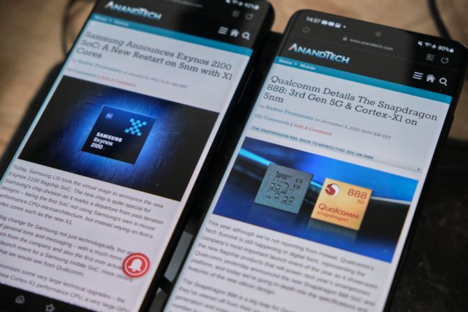
The new Galaxy S21 series of devices have been out commercially for a week now, and we’ve managed to get our hands on two Galaxy S21 Ultras – one with Qualcomm’s new Snapdragon 888 SoC, and one with Samsung’s new Exynos 2100 SoC. Both chipsets this year are more similar than ever, both now sporting similar CPU configurations, and both being produced on a new Samsung 5nm (5LPE) process node.
Ahead of our full device review of the Galaxy S21 Ultra (and the smaller Galaxy S21), today we’re focusing on the first test results of the new generation of SoCs, putting them through their paces, and pitting them against each other in the new 2021 competitive landscape.
The Snapdragon 888
| Qualcomm Snapdragon Flagship SoCs 2020-2021 | |||
| SoC | Snapdragon 865 |
Snapdragon 888 |
|
| CPU | 1x Cortex-A77 @ 2.84GHz 1x512KB pL2 3x Cortex-A77 @ 2.42GHz 3x256KB pL2 4x Cortex-A55 @ 1.80GHz 4x128KB pL2 4MB sL3 |
1x Cortex-X1 @ 2.84GHz 1x1024KB pL2 3x Cortex-A78 @ 2.42GHz 3x512KB pL2 4x Cortex-A55 @ 1.80GHz 4x128KB pL2 4MB sL3 |
|
| GPU | Adreno 650 @ 587 MHz | Adreno 660 @ 840MHz | |
| DSP / NPU | Hexagon 698 15 TOPS AI (Total CPU+GPU+HVX+Tensor) |
Hexagon 780 26 TOPS AI (Total CPU+GPU+HVX+Tensor) |
|
| Memory Controller |
4x 16-bit CH @ 2133MHz LPDDR4X / 33.4GB/s or @ 2750MHz LPDDR5 / 44.0GB/s 3MB system level cache |
4x 16-bit CH @ 3200MHz LPDDR5 / 51.2GB/s 3MB system level cache |
|
| ISP/Camera | Dual 14-bit Spectra 480 ISP 1x 200MP or 64MP with ZSL or 2x 25MP with ZSL 4K video & 64MP burst capture |
Triple 14-bit Spectra 580 ISP 1x 200MP or 84MP with ZSL or 64+25MP with ZSL or 3x 28MP with ZSL 4K video & 64MP burst capture |
|
| Encode/ Decode |
8K30 / 4K120 10-bit H.265 Dolby Vision, HDR10+, HDR10, HLG 720p960 infinite recording |
8K30 / 4K120 10-bit H.265 Dolby Vision, HDR10+, HDR10, HLG 720p960 infinite recording |
|
| Integrated Modem | none (Paired with external X55 only) (LTE Category 24/22) DL = 2500 Mbps 7x20MHz CA, 1024-QAM UL = 316 Mbps 3x20MHz CA, 256-QAM (5G NR Sub-6 + mmWave) DL = 7000 Mbps UL = 3000 Mbps |
X60 integrated (LTE Category 24/22) DL = 2500 Mbps 7x20MHz CA, 1024-QAM UL = 316 Mbps 3x20MHz CA, 256-QAM (5G NR Sub-6 + mmWave) DL = 7500 Mbps UL = 3000 Mbps |
|
| Mfc. Process | TSMC 7nm (N7P) |
Samsung 5nm (5LPE) |
|
Starting off with the new Snapdragon 888 SoC, Qualcomm’s new flagship model makes iterative steps this generation, with the biggest changes of the new design actually being in the form of the new Hexagon 780 accelerator, which fuses together traditional scalar and vector DSP operations with tensor execution engines within one single IP block.
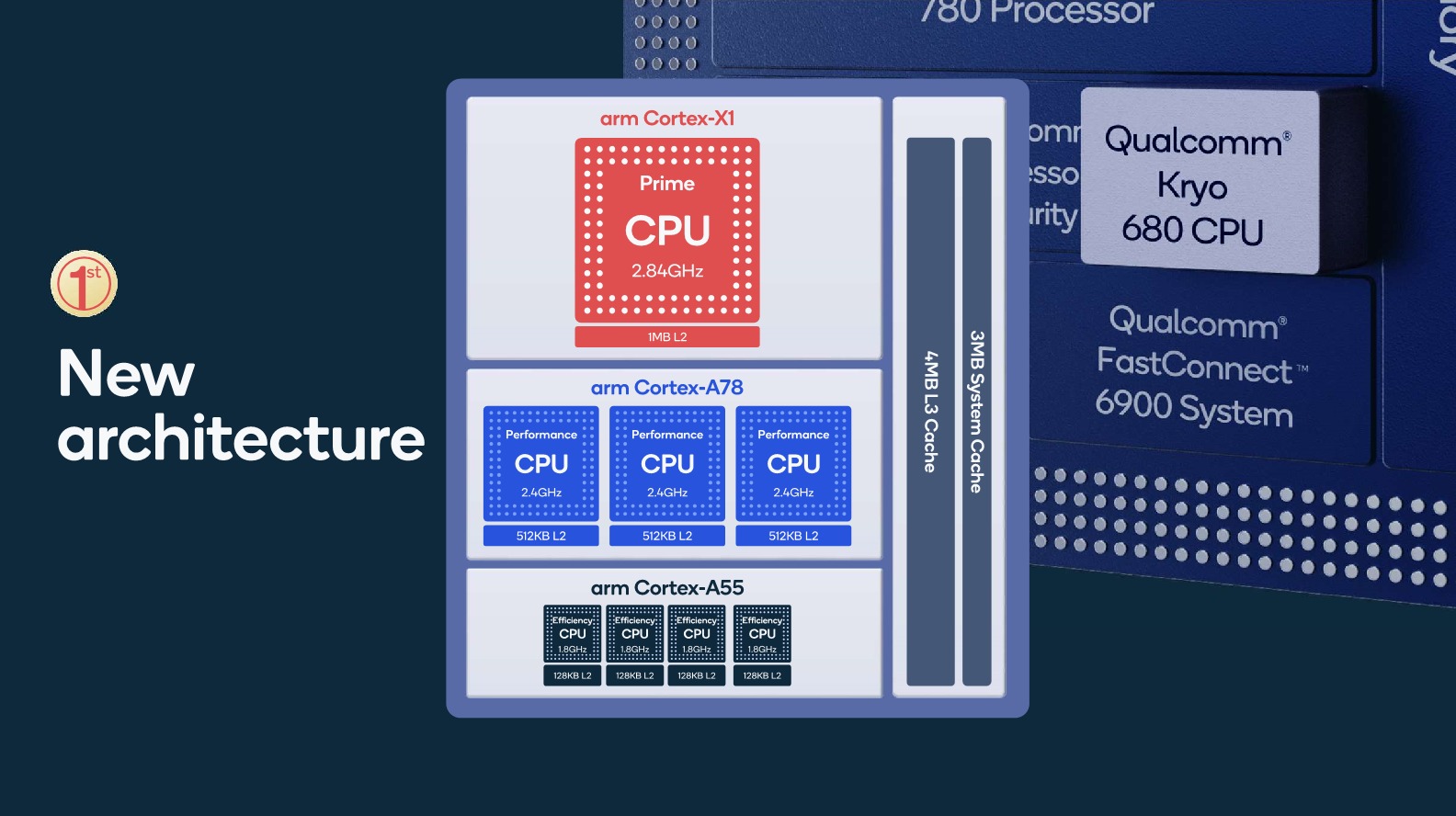
Of course, we’re also seeing upgrades elsewhere in the architecture, with the Snapdragon 888 being among the first SoCs to use Arm’s new Cortex-X1 CPU IP, promising large performance gains relative to last generation Cortex-A77 cores. The single X1 cores in the Snapdragon 888 clocks in at 2.84GHz – the same as the previous generation Snapdragon 865’s prime Cortex-A77 cores, and less than the 3.1GHz and 3.2GHz Snapdragon 865+ and recently announced Snapdragon 870 SoCs.
Alongside the X1, we find three Cortex-A78 cores at 2.42GHz, again the same clocks as the previous generation 865 SoCs, but this time around with double the L2 caches at 512KB.
The Cortex-A55 little cores remain identical this generation, clocking in at 1.8GHz.
Although we had been expecting 8MB L3 cache flagship SoCs this year, it does look like Qualcomm opted to remain at 4MB for this generation – but at least the company dons the X1 core with the maximum 1MB L2 cache configuration.
On the GPU side of things, Qualcomm’s new Adreno 660 GPU now clocks in up to a peak 840MHz – a whopping 43% higher frequency than the Snapdragon 865 GPU. The company’s performance claims here are also astonishing, promising a +35% boost in performance. We’ll have to see how this all ends up in terms of power consumption and long-term performance in the later dedicated GPU section.
What’s quite different for the Snapdragon 888 this year is that Qualcomm has moved from a TSMC N7P process node to Samsung’s new 5LPE node – the generally wildcard in this whole situation as we haven’t had any prior experience with this new 5nm node.
The Exynos 2100
| Samsung Exynos SoCs Specifications | ||
| SoC |
Exynos 990 |
Exynos 2100 |
| CPU | 2x Exynos M5 @ 2.73GHz 2MB sL2 3MB sL3 2x Cortex-A76 @ 2.50GHz 2x256KB pL2 4x Cortex-A55 @ 2.00GHz 4x64KB pL2 1MB sL3 |
1x Cortex-X1 @ 2.91GHz 1x512KB pL2 3x Cortex-A78 @ 2.81GHz 3x512KB pL2 4x Cortex-A55 @ 2.20GHz 4x64KB pL2 4MB sL3 |
| GPU | Mali G77MP11 @ 800 MHz | Mali G78MP14 @ 854 MHz |
| Memory Controller |
4x 16-bit CH @ 2750MHz LPDDR5 / 44.0GB/s 2MB System Cache |
4x 16-bit CH @ 3200MHz LPDDR5 / 51.2GB/s 6MB System Cache |
| ISP | Single: 108MP Dual: 24.8MP+24.8MP |
Single: 200MP Dual: 32MP+32MP (Up to quad simultaneous camera) |
| NPU | Dual NPU + DSP + CPU + GPU 15 TOPs |
Triple NPU + DSP + CPU + GPU 26 TOPs |
| Media | 8K30 & 4K120 encode & decode H.265/HEVC, H.264, VP9 |
8K30 & 4K120 encode & 8K60 decode H.265/HEVC, H.264, VP9 AV1 Decode |
| Modem | Exynos Modem External (LTE Category 24/22) DL = 3000 Mbps 8x20MHz CA, 1024-QAM UL = 422 Mbps ?x20MHz CA, 256-QAM (5G NR Sub-6) DL = 5100 Mbps (5G NR mmWave) DL = 7350 Mbps |
Exynos Modem Integrated (LTE Category 24/18) DL = 3000 Mbps 8x20MHz CA, 1024-QAM UL = 422 Mbps 4x20MHz CA, 256-QAM (5G NR Sub-6) DL = 5100 Mbps UL = 1920Mbps (5G NR mmWave) DL = 7350 Mbps UL = 3670 Mbps |
| Mfc. Process | Samsung 7nm (7LPP) |
Samsung 5nm (5LPE) |
On the Samsung LSI side of things, we find the brand-new Exynos 2100. Unlike the Snapdragon 888’s more incremental changes in terms of SoC design, the new Exynos is a rather large departure for Samsung’s SoC division as this is the first flagship design in many years that no longer uses Samsung’s own in-house CPU microarchitecture, but rather reverts back to using Arm Cortex cores, which in this case is also the new Cortex-X1 and Cortex-A78 cores.
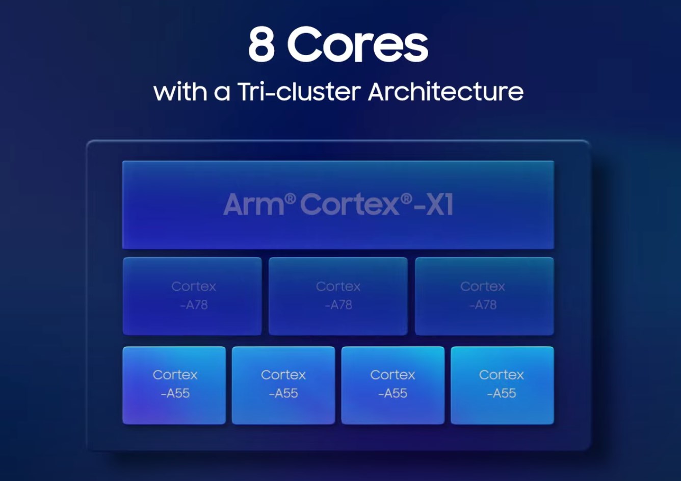
From a high-level, the CPU configuration of the Exynos 2100 looks nigh identical to that of the Snapdragon 888, as both are 1+3+4 designs with X1, A78 and A55 cores. The differences are in the details:
The X1 cores on the Exynos 2100 clock slightly higher at up to 2.91GHz, while the Cortex-A78 clock in significantly higher than the Snapdragon as they reach 2.81GHz. The Cortex-A55 cores are also quite aggressive in terms of frequency as they now reach 2.20GHz – so overall across the board higher clocks than the Snapdragon variant.
Where the Exynos isn’t as aggressive though is in its cache configurations. Most importantly, the X1 cores here only feature 512KB of L2 cache, which is a bit weird given the all-out-performance philosophy of the new CPU. The Cortex-A78s also see the usage of 512KB L2 caches, while the little A55 cores feature 64KB L2’s – less than the Snapdragon counterparts.
Much like the Snapdragon, the L3 cache also falls in at 4MB rather than the 8MB we would have hoped for this generation, however Samsung does surprise us with the usage of an estimated 6-8MB system level cache, up from the 2MB design in the Exynos 990.
On the GPU side of things, we see a Mali-G78MP14 at up to 854MHz. That’s 27% more cores and 6.7% higher frequency, and the company is also boasting massive performance gains as it touts a 40% generational improvement.
Let them fight
In today piece, we’ll be mostly focusing around CPU and GPU performance, as an especially interesting comparison will be to see how the two designs do against each other, given that they both now use Arm’s newest Cortex-X1 cores and both are sporting the same manufacturing node.
The GPU comparisons will also be interesting – and maybe quite controversial, as the results won’t be what many people will have been expecting.
While we would have liked to showcase AI performance of the two SoCs – unfortunately the software situation on the Galaxy S21’s right now means that neither SoC are fully taking advantage of their new accelerators, so that’s a topic to revisit in a few months’ time once the proper frameworks have been updated by Samsung.


123 Comments
View All Comments
Andrei Frumusanu - Tuesday, February 9, 2021 - link
I don't have 5G coverage here so it's not feasible for me to test.Edwardmcardle - Wednesday, February 10, 2021 - link
Will you be testing reception differences e.g. 4g and wifi? Fantastic write up as always!Dorkaman - Tuesday, February 9, 2021 - link
Different s21 ultra phones can have different performance says tech chaphttps://youtu.be/yuNNmf2gIRc
I guess this is due to binning and his tests show his Exonys 2100 is in the middle. Strange. Also, the battery life is better on the 888 and external temps are about the samd.
serendip - Tuesday, February 9, 2021 - link
All this really doesn't look good for Windows on ARM if we're stuck with hot and hungry Qualcomm chips on Samsung 5nm. The 8cx and SQ on TSMC 7nm were very efficient but that's with slower A76 cores. I'm hoping a quad-X1 design on TSMC 5nm will be in the next iteration of the Surface Pro X or Galaxy Book S.Raqia - Tuesday, February 9, 2021 - link
Disappointing sustained performance, however the S21 series lacks the phase change vapor chamber cooling solution of the S20's:https://9to5google.com/2021/01/18/samsung-galaxy-s...
vs
https://www.ifixit.com/News/43501/why-samsung-buil...
Notably the Mi11 has this:
https://gadgettendency.com/a-triple-chamber-as-a-s...
This makes for better subsequent runs but the SoCs built on 5LPE are still disappointing.
iphonebestgamephone - Wednesday, February 10, 2021 - link
Mi 11 may have the vapor chamber for better cooling, but it also allows for a higher battery temperature. If they throttled at the same temps we could see how useful that thing actually is.dudedud - Wednesday, February 10, 2021 - link
Not all S20s had that vapor chamber. Some just had a graphene layer, which in theory would give similar results. Don't know if the S21 uses graphene tho.darkich - Wednesday, February 10, 2021 - link
The battery life benchmarks are indication of how actually invalid the whole Anantech's premise is.Pretty much ALL actual real usage tests have shown BIG improvements in the autonomy between the S20/S21 yet Andrei wants us to believe in the stupid benchmark test that shows "regression" between Exynos 990 and Exynos 2100.
What a joke..
ChrisGX - Sunday, February 14, 2021 - link
I would say these results are incomplete rather than invalid. The PCMark Work 2.0 - Battery Life test is a demanding mixed usage benchmark. When running that benchmark it isn't exactly a shock that the Exynos 2100 S21 Ultra should return very slightly reduced battery life than the Exynos 990 S20 Ultra. Anandtech isn't alone in noting that when processing demanding workloads the Exynos 2100 draws more power (on average) than the Exynos 990. Andrei, for his part, is explicit that the Exynos 2100 is also significantly more performant than its predecessor. He does say that the increased performance wasn’t just achieved through improved efficiency, but also through greater power usage and it is hard to dispute that looking at the numbers.There is a gap in the data however. The full PCMark Work 2.0 - Battery Life test involves a Work performance score that gives a more complete picture of how much work/the rate that work is being completed while executing the test. That would be very useful information to have. Still, it is undoubtedly the case that the reduction in battery life that Andrei mentions is not due to a regression but rather the increased rate that the Exynos 2100 is executing work (when processing demanding mixed usage workloads). While that information isn't provided in connection to the PCMark Work 2.0 - Battery Life test the GFXBench GPU heavy test data (arranged in Power Efficiency tables) does confirm the high power draw of the Exynos 2100 during peak performance bursts (which must bump up average power consumption as well) even as that chip roundly outperforms the Exynos 990.
Indeed, heavy mixed usage workloads are not going to put the Exynos 2100 battery life in the best light. Still, Andrei did show the results from a Web Browsing Battery Life test that undoubedly will be useful to a lot of phone users who don't view the results of the PCMark Work 2.0 - Battery Life test as having a lot of relevance for them. But, I, for one, am happy to have that information.
Andrei seems to be adding to/reworking the battery life data in this review.
https://benchmarks.ul.com/pcmark-android
https://s3.amazonaws.com/download-aws.futuremark.c...
sachouba - Wednesday, February 10, 2021 - link
Nice peak power consumption!It doesn't seem unlikely that we'll end up with a situation similar to Apple's battery gate on Snapdragon 888 devices, in a few years. Way to go!