Intel's Process Roadmap to 2025: with 4nm, 3nm, 20A and 18A?!
by Dr. Ian Cutress on July 26, 2021 5:00 PM ESTNew Technology Features for 2024: RibbonFETs
One of the major features of this roadmap is highlighted when it shifts to 20A, Intel’s process name referring to Angstroms rather than nanometers. At this juncture, as mentioned above, Intel will be transitioning from its FinFET design over to a new type of transistor, known as a Gate-All-Around transistor, or GAAFET. In Intel’s case, the marketing name they are giving their version is RibbonFET.
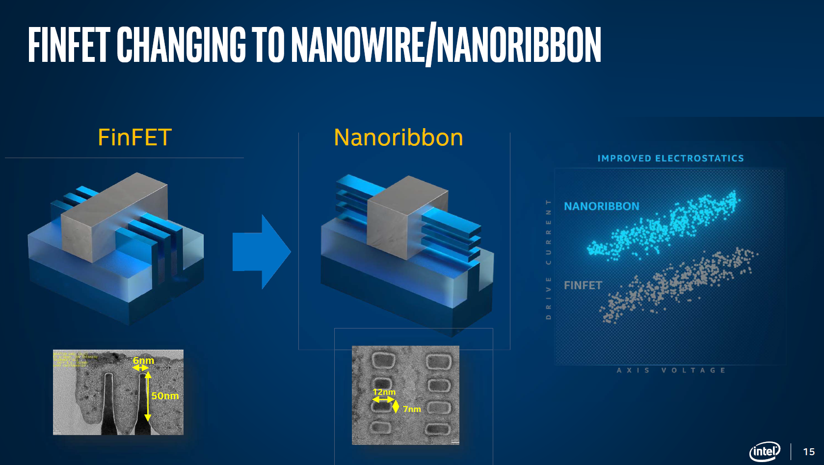
It has been widely expected that once the standard FinFET runs out of steam that the semiconductor manufacturing industry will pivot to GAAFET designs. Each of the leading edge vendors call their implementation something different (RibbonFET, MBCFET), but it is all using the same basic principle – a flexible width transistor with a number of layers helping drive transistor current. Where FinFETs relies on multiple quantized fins for source/drain and a cell height of multiple tracks of fins, GAAFETs enable a single fin of variable length, allowing the current for each individual cell device to be optimized in power, performance, or area.
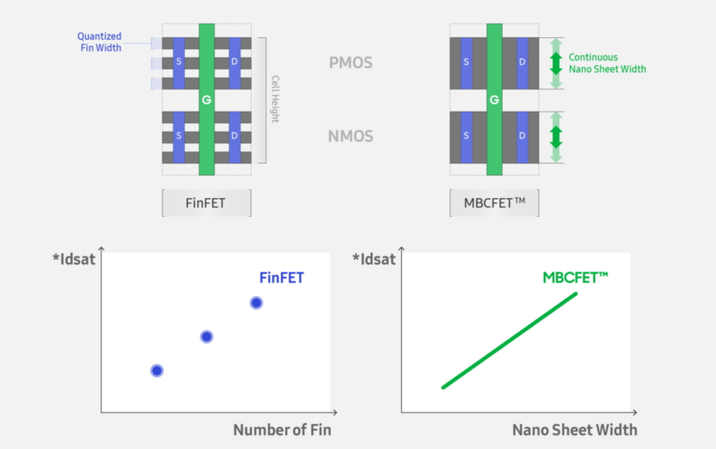
Image from Samsung
Intel has been discussing GAAFETs in technical semiconductor conferences for a number of years, at the International VLSI conference in June 2020, then CTO Dr. Mike Mayberry showcased a diagram with the enhanced electrostatics of moving to a GAA design. At the time we asked about Intel’s timescale for implementing GAA in volume, and were told to expect them ‘within 5 years’. At present Intel’s RibbonFET is due to come with the 20A process, likely to be productized by the end of 2024 based on the roadmaps outlined above.
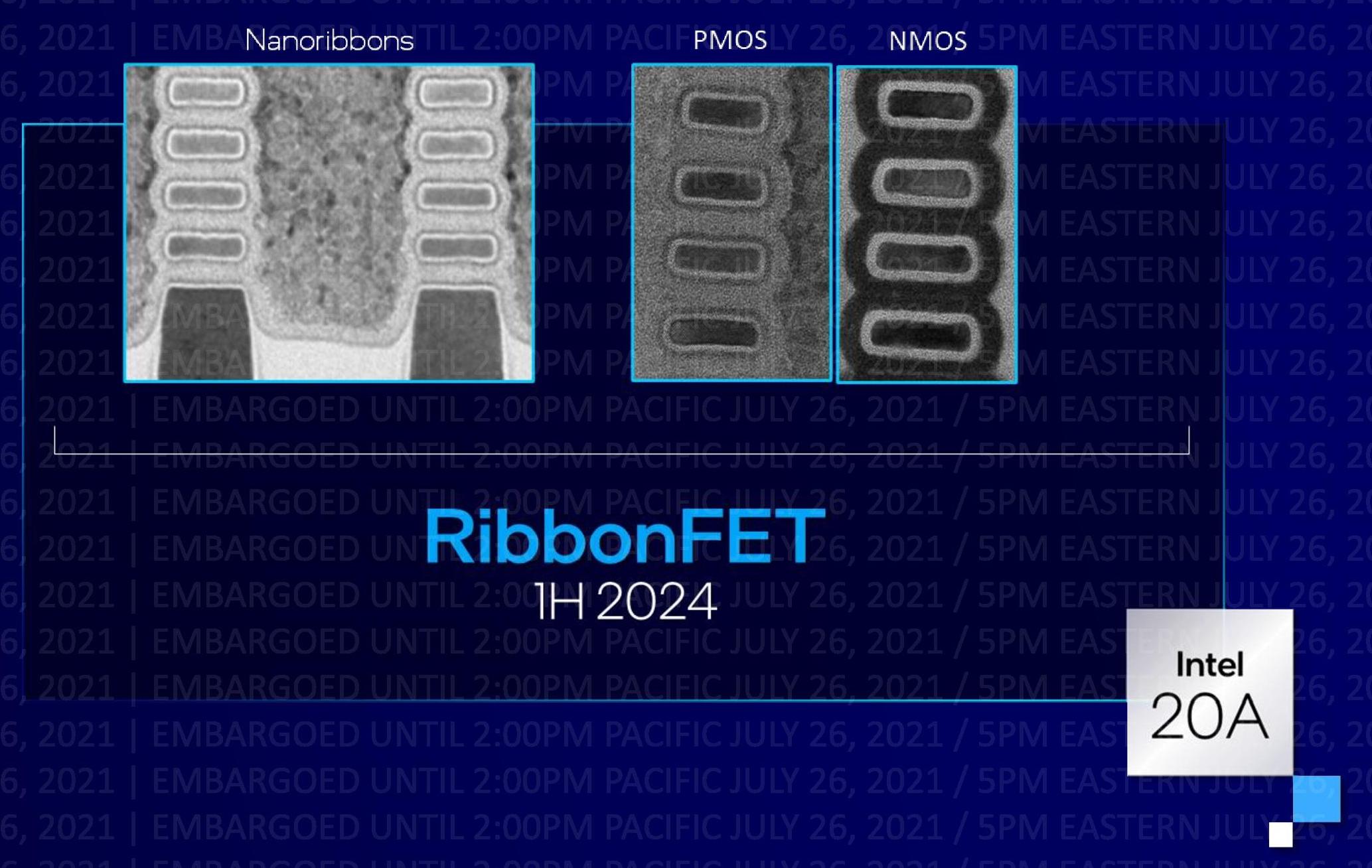
In Intel’s RibbonFET diagrams for this event, they’re showing both PMOS and NMOS devices, as well as what clearly looks like a 4-stack design. Given that I have seen presentations from Intel involving anything from 2-stack to 5-stack at the industry conferences, we confirmed that Intel will indeed be using a 4-stack implementation. The more stacks that are added, the more process node steps are required for manufacturing, and to quote Intel’s Dr. Kelleher, ‘it’s easier to remove a stack than to add one!’. Exactly what is the right number of stacks for any given process or function is still an active area of research, however Intel seems keen on four.
In comparison with Intel’s competitors,
TSMC is expected to transition to GAAFET designs on its 2nm process. At its annual Tech Symposium in August 2020, TSMC confirmed that it would remain on FinFET technology all the way to its 3nm (or N3) process node as it has been able to find significant updates to the technology to allow performance and leakage scaling beyond what was initially expected – N3 is quoted to have up to a 50% performance gain, 30% power reduction, or 1.7x density gain over TSMC N5. Staying on FinFETs, TSMC stated, provides comfort to its customers. Details on TSMC’s N2 have not been disclosed.
Samsung by contrast has stated that it will be introducing its GAA technology with its 3nm process node. Back in Q2 2019, Samsung Foundry announced the first v0.1 development kit of its new 3GAE process node using GAAFETs was being made available to key customers. At the time Samsung predicted volume production by end of 2021, and the latest announcement suggests that while 3GAE will deploy in 2022 internally, main customers may have to wait until 2023 for its more advanced 3GAP process.
To put this into a table:
| Gate-All-Around Transistor Deployment | |||
| AnandTech | Name | Process | Timeframe |
| Intel | RibbonFET | 20A | 2024 |
| 18A | 2025 | ||
| TSMC | GAAFET | N2 / 2nm | EoY 2023? |
| Samsung | MBCFET | 3GAE | 2022 |
| 3GAP | 2023 | ||
By this metric, Samsung might be first to the gate, albeit with an internal node, while TSMC is going to get a lot out of its N5, N4, and N3 nodes first. Around end of year 2023 is when it gets interesting as TSMC may be looking at its N2 designs, while Intel is committed to that 2024 timeframe. The official slide says first half 2024, though as a technology announcement vs product announcement, there is often some lag between the two.
New Technology Features for 2024: PowerVias
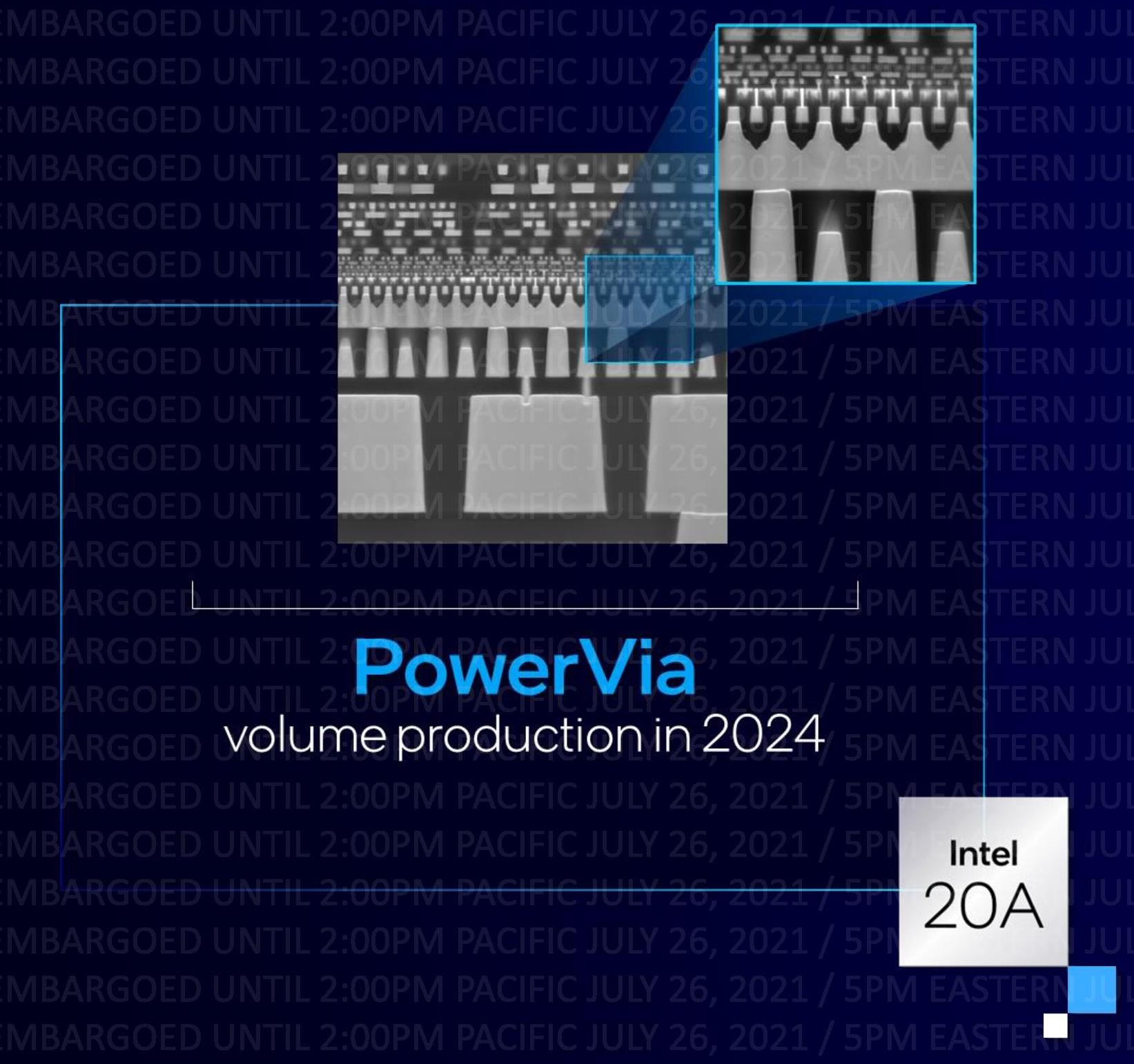
The other arm of Intel’s 20A designs in 2024 is what the company is calling ‘PowerVia’. The concept here pivots the traditional understanding of chip design from a multi-layered cake into a sandwich of sorts.
The manufacturing process of a modern circuit starts the transistor layer, M0, as the smallest layer. Above that, additional metal layers are added at increasing sizes to account for all the wiring needed between the transistors and different parts of the processor (cache, buffers, accelerators). A modern high-performance processor typically has anywhere from 10 to 20 metal layers in its design, with the top layer where the external connections are placed. The chip is then flipped over (known as flip chip) so that the chip can talk to the outside world with those connections on the bottom, and the transistors at the top.
With PowerVias, we now put the transistors in the middle of the design. On one side of the transistors we put the communication wires that allow parts of the chip to talk to each other. On the other side are all the power related connections (along with power gating control). In essence, we moved to a sandwich where the transistors are the filling. This is usually referred to as ‘backside power delivery’ in the industry – PowerVia is Intel’s marketing name.
From a holistic level, we can ascertain that the benefits of this design start with simplifying both the power and the connectivity wires. Typically these have to be designed to ensure there is no signaling interference, and one of the big sources of interference are large power carrying wires, so this takes them out of the equation by putting them on the other side of the chip. It also works the other way – the interference of the interconnected data wires can increase the power delivery resistance, resulting in lost energy and thermals. In this way, PowerVias can help new generations of transistors as drive currents increase by having the power directly there, rather than routed around the connectivity.
There are a couple of hurdles here to mention however. Normally we start manufacturing the transistors first because they are the most difficult and most likely to have defects – if a defect is caught early in the metrology (defect detection in manufacturing), then that can be reported as early in the cycle as possible. By having the transistors in the middle, Intel would now be manufacturing several layers of power first before getting to the tough bit. Now technically these layers of power would be super easy compared to the transistors, and nothing is likely to go wrong, but it is something to consider.
The second hurdle to think about is power management and thermal conductivity. Modern chips are built transistor first into a dozen layers ending with power and connections, and then the chip is flipped, so the power hungry transistors are now at the top of the chip and the thermals can be managed. In a sandwich design, that thermal energy is going to go through whatever ends up on the top of the chip, which is most likely going to be the internal communication wires. Assuming that the thermal increase of these wires doesn’t cause any issues in production or regular use, then perhaps this isn’t so much of an issue, however it is something to consider when heat has to be conducted away from the transistors.
It is worth noting that this ‘backside power delivery’ technology has been in development for a number of years. Across five research papers presented at the VLSI symposium in 2021, imec presented several papers on the technology showing recent advancements when using FinFETs, and in 2019 Arm and imec announced similar technology on an Arm Cortex-A53 built on an equivalent 3nm process in imec’s research facilities. Overall the technology reduces the IR drop on the design, which is becoming increasingly harder to achieve on more advanced process node technologies to drive performance. It will be interesting to see the technology when it is in high volume on high performance processors.


326 Comments
View All Comments
TheinsanegamerN - Tuesday, July 27, 2021 - link
Oh look, the reddit crybabies are leaking onto anandtech nowNow see, THAT was an ad hominem.
Machinus - Tuesday, July 27, 2021 - link
redditards should be put into a playpen away from other websitesSpunjji - Thursday, July 29, 2021 - link
@Machinus - maybe don't use slurs against other people's intelligence when you managed to fatally misread not one, but two replies to your comments.You were shown two examples that logically counter your claim that a comeback is "impossible", and your response was to mock the person for pointing out the indisputable fact that those comebacks were considered exceedingly unlikely *before they happened*.
You are in effect identifying yourself as someone who would have thought those things back then, given that you are arguing so passionately that it's true about Intel now.
Machinus - Thursday, July 29, 2021 - link
fatally? Were they fatal?This comeback is impossible. read my comments that already explained why you're wrong. :)
Spunjji - Friday, July 30, 2021 - link
@Machinus - fatal for your argument, absolutely. I thought that was implicit, but this appears to be a game where you misread everything and then insist you're smarter than everyone else.Your comments didn't "explain" anything, they made inaccurate assertions.
Machinus - Tuesday, August 3, 2021 - link
No, my comments were excellent, unlike the tripe appearing next to your username.mode_13h - Tuesday, July 27, 2021 - link
> anything can happen between now and 2025.Yeah, like China could take back Taiwan. Then, it would be largely irrelevant how good TSMC is. AMD would have to go cap-in-hand to IFS and beg for some capacity.
Lord of the Bored - Tuesday, July 27, 2021 - link
Taiwan's the older of the two. Taiwan didn't split, the communists just never conquered them."The communist regime could finish their conquest of China." would be more historically accurate.
mode_13h - Wednesday, July 28, 2021 - link
> the communists just never conquered them.Well, sure. If you're only going that far back. But, according to Wikipedia:
"Qing dynasty formally annexed Taiwan, placing it under the jurisdiction of Fujian province."
Anyway, you seem to get my point. Not that I want to see that happen, but its likelihood has certainly been increasing in recent years.
Threska - Wednesday, July 28, 2021 - link
Japan might want to get in on this, along with a few other countries.