Qualcomm Announces Snapdragon 8+ Gen 1: Moving to TSMC for More Speed, Lower Power
by Ryan Smith on May 20, 2022 8:00 AM EST
As the dark of the night rolls into China this evening, Qualcomm is hosting a mobile-focused product launch event they’re calling “Snapdragon Night”. Headlining the event is the announcement of the company’s new flagship SoC, the Snapdragon 8+ Gen 1. A mid-generation update to their flagship smartphone SoC, the Snapdragon 8 Gen 1, the 8+ Gen 1 follows Qualcomm’s annual tradition of releasing a refresh product to boost performance and to give partners something new to work with for the second half of the year. And for this year in particular, we’re looking at a very notable change in chips from Qualcomm.
Unlike previous generations where Qualcomm merely launched a faster speed bin of their existing silicon, for 2022 we have something more substantial to talk about. Qualcomm has switched up foundries entirely – moving from Samsung to TSMC – and as a result is rolling out a new die. Thanks to this, the Snapdragon 8+ Gen 1 Qualcomm is reaping something of a one-off manufacturing gain, allowing them to both dial up CPU and GPU performance while simultaneously cutting power consumption.
| Qualcomm Snapdragon 8 Gen 1 Flagship SoCs | |||
| SoC | Snapdragon 8+ Gen 1 | Snapdragon 8 Gen 1 | |
| CPU | 1x Cortex-X2 @ 3.2GHz 3x Cortex-A710 @ 2.8GHz 4x Cortex-A510 @ 2.0GHz 6MB sL3 |
1x Cortex-X2 @ 3.0GHz 3x Cortex-A710 @ 2.5GHz 4x Cortex-A510 @ 1.8GHz 6MB sL3 |
|
| GPU | Adreno (10% Higher Clockspeed) |
Adreno | |
| DSP / NPU | Hexagon | Hexagon | |
| Memory Controller |
4x 16-bit CH @ 3200MHz LPDDR5 / 51.2GB/s 4MB system level cache |
||
| ISP/Camera | Triple 18-bit Spectra ISP 1x 200MP or 108MP with ZSL or 64+36MP with ZSL or 3x 36MP with ZSL 8K HDR video & 64MP burst capture |
||
| Encode/ Decode |
8K30 / 4K120 10-bit H.265 Dolby Vision, HDR10+, HDR10, HLG 720p960 infinite recording |
||
| Integrated Modem | X65 integrated (5G NR Sub-6 + mmWave) DL = 10000 Mbps UL = 3000 Mbps |
||
| Mfc. Process | TSMC 4nm | Samsung 4nm | |
Quickly diving into the specifications, the new Snapdragon 8+ Gen 1 is essentially the original Snapdragon 8 Gen 1 ported over from Samsung’s 4nm line over to one of TSMC’s 4nm lines. Under more normal circumstances, this kind of a shift would likely be unremarkable – or at most, an amusing exercise in looking for edge cases – however for Qualcomm’s flagship SoC, the matter is more significant.
While official sources and statements on the quality of Samsung’s 4nm process are few and far between, unofficially, it’s become clear that Samsung’s 4nm process hasn’t lived up to expectations. This has caused a cascading impact on the chips made on the process node, leading to the original Snapdragon 8 Gen 1 developing an affinity for power consumption, and Samsung’s own Exynos 2200 not faring any better. Conversely, by all accounts TSMC’s N4 process is looking great, with the optically shrunk node building off of TSMC’s already successful and very performant 5nm technologies.
As a result of this performance gap between Samsung and TSMC’s 4nm nodes, Qualcomm is taking the unusual step of (essentially) porting their high-end SoC over to TSMC’s fab. Which, although not strictly necessary – Qualcomm carries a lot of momentum and the 8 Gen 1 has been selling well – is certainly a prudent move for the company. Qualcomm is facing especially stiff competition this generation from MediaTek, whose flagship-level Dimensity 9000 SoC was the lead product for TSMC’s 4nm node. And that leaves MediaTek with a distinct advantage against the original 8 Gen 1, one that Qualcomm would be very happy to nullify.
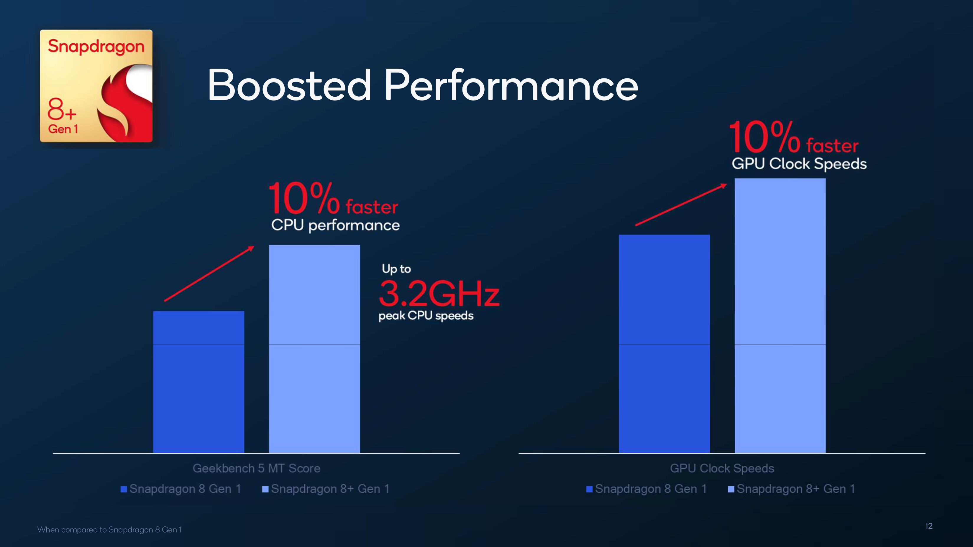
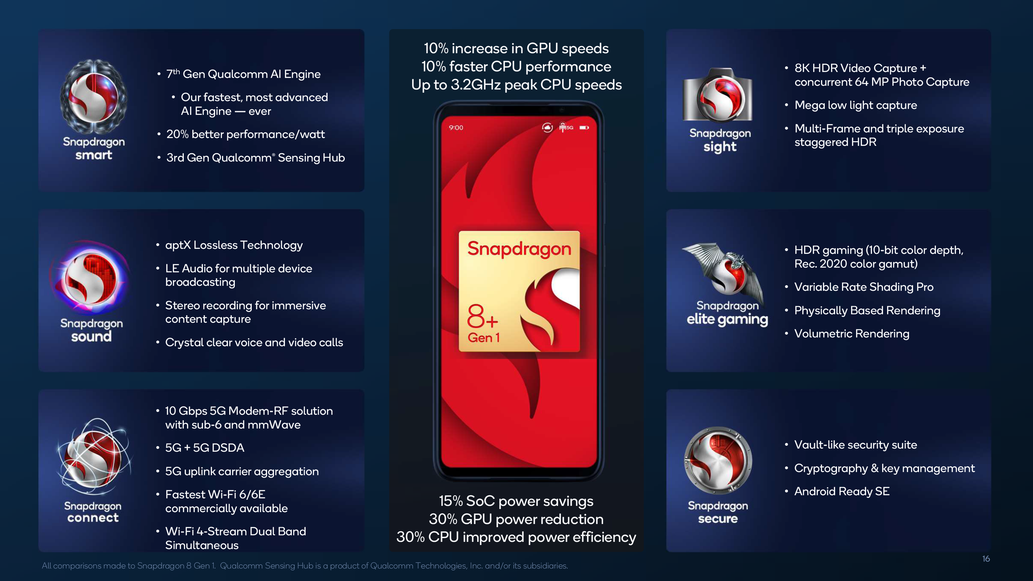
Ultimately, the switch in fabs is giving Qualcomm a chance to improve upon the original 8 Gen 1 from both ends of the spectrum, resulting in the Snapdragon 8+ Gen 1. On the performance front, TSMC’s node affords them an easy opportunity to increase CPU and GPU clockspeeds for more performance. The prime Cortex-X2 core is now clocked 7% higher, at 3.2GHz, and meanwhile the A710 and A510 clusters have seen their clockspeeds dialed up even more significantly, by around 12% each. Now even the slowest A510 cores can run at 2GHz. GPU clockspeeds have also been similarly increased, and while Qualcomm does not disclose specific clockspeeds there, they have confirmed that the 8+ Gen 1’s Adreno GPU block is clocked 10% higher than the original 8 Gen 1.
But, if anything, the bulk of Qualcomm’s gains from the switch in manufacturing nodes are being invested in cutting power consumption. Something of a sore point with the 8 Gen 1, TSMC’s better 4nm process means that Qualcomm is seeing much lower power consumption across their SoC at iso-frequency.
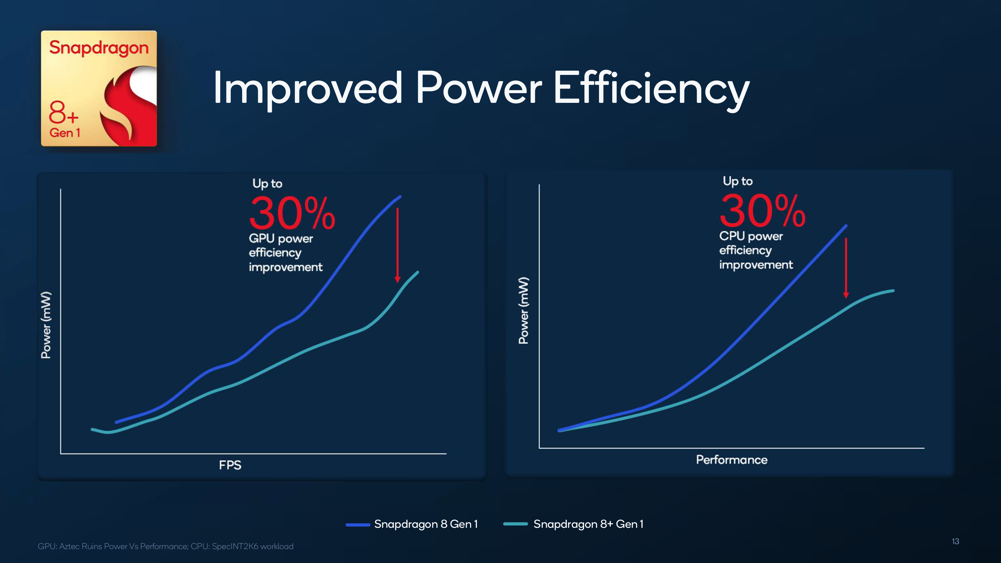
Officially, Qualcomm is claiming a 30% improvement in both GPU and CPU power efficiency. Though as mentioned before, this is at iso-frequency and doesn’t take into account the higher peak clockspeeds of the 8+ Gen 1. Consequently, the real-world power savings aren’t going to be quite as great on a peak-to-peak basis, but according to Qualcomm the power savings are still significant. Overall, the company is touting a 15% reduction in SoC power usage under “practical usage patterns” versus the original 8 Gen 1, which in turn should lead to improved battery lifetimes in handsets that adopt the new SoC.
Past that, the official specifications for the 8+ Gen 1 do not reflect any material changes to the SoC’s configuration versus the original chip. So we’re still looking at the same integrated X65 5G modem, the same Spectra ISP, and the same video encode/decode blocks (sorry, gang, still no AV1 support!). So, despite assembling a new die for their mid-generation refresh product this year, there aren’t any new features to speak of with the 8+ Gen 1.
As for SoC performance, officially Qualcomm is claiming 10% improved GPU and CPU performance, owing to those aforementioned clockspeed increases. While we weren’t able to attend a benchmarking session that Qualcomm held last week, the Performance Mode figures being released by the company are roughly in-line with these claims. Qualcomm’s Geekbench 5 results are several percent higher than what we benchmarked back in December at the 8 Gen 1 launch event, though it’s notable that they didn’t achieve meaningfully higher scores in PCMark. GPU performance figures are similarly mixed, with some of Qualcomm’s official results coming very close to our original 8 Gen 1 results, but I’m reluctant to read too much into them given how much if a difference peak versus sustained testing makes in GPU results. As always, the final word will need to come down to independent, third-party testing, though at face value nothing Qualcomm claims is unreasonable given the clockspeed improvements and the thermal headroom gained from the switch to TSMC.
Finally, as for consumers, they’ll be able to get their first look at Snapdragon 8+ Gen 1 devices in Q3 of this year. According to Qualcomm, many of the usual suspects have signed on to release phones based on the new SoC, including Asus, Motorola, OnePlus, Honor, and Xiaomi.


51 Comments
View All Comments
ChrisGX - Tuesday, May 31, 2022 - link
No, the naming conventions are clear. The generation number has no qualifiers and the chip series number has three: 'c' indicating 'compute' (for laptop chips etc.), 'x' indicating 'extreme' (which might suggest a major upgrade to the GPU over the standard part ot something of that order) and '+' which indicates, well, 'plus' (pushed clockrates, for instance, rather than any architectural changes from the standard part). (Note: While Qualcomm already has 'cx' chips I doubt we will ever see an 'x+' or 'cx+' parts.)The greater significance of this naming scheme seems to be that Qualcomm is intending to cut down on the total number of chip variations. If you just name the chip series, without some extended chip name like 'Snapdragon 778G' or 'Snapdragon 888', say, then you have effectively limited the chip variations that might ship with those designators. So, 'Snapdragon 7' or 'Snapdragon 8' plus a small numbers of qualifiers doesn't allow for a lot of variation. Also, within any generation of a chip all variation will be indicated by that chip series number and the mentioned qualifiers. Will Qualcomm continue to create consistent chip names? Time will tell.
SydneyBlue120d - Friday, May 20, 2022 - link
When can we expect the first Qualcomm SOC made by Intel?Dante Verizon - Friday, May 20, 2022 - link
Late 2033*syxbit - Friday, May 20, 2022 - link
Why does this matter?The most important device to use the 8 Gen 1 is the Galaxy S22, and that's already shipped. THe new Pixel won't have this either. So is it just a couple of gamer phones?
iphonebestgamephone - Saturday, May 21, 2022 - link
Ultra phones from some chinese brands, xiaomi oneplus etc.hnlog - Monday, May 23, 2022 - link
Galaxy (Z) Fold4name99 - Friday, May 20, 2022 - link
What does sL3 mean?- shared L3? (ie shared across all CPUs, so like every L3 ever pretty much)
- synthetic L3 (ie data stored in other L2's can be used by a particular CPU via sideways transfers, ala IBM)?
- something else?
Ryan Smith - Monday, May 23, 2022 - link
You had it right with "shared L3"erotomania - Friday, May 20, 2022 - link
5800X3D? Final writeup?xol - Friday, May 20, 2022 - link
Feels like Samsung has been struggling post 8nm.Apart from a few Snapdragons I'm not sure what non Exynos IP they've made.
The supposed 780G (5nm) is almost completly MIA, especially when compared to the widely used 778 (6nm TSMC) . and their 888 was sometimes shown to be no better than the (cheaper and 7nm TSMC) 870 just because it thermally throttle before any extra performance could be got out of it - outside short term burst use.
Not aware of a single order Mediatek has given them in the same period.
Plus these comparisons with TSMC's 'equivalent' 4nm process makes Samsung look like a half node behind. Not a good look.
afaik the actual foundry financials are hidden and not separated from their flash/DRAM business which is surely the source of that divisions massive market share/profits.
Hopefully they will make a massive comeback at some point .. maybe first to GAAFET ? (Just like Intel went from paper launching 10nm for over a year to releasing the excellent Alder Lake chips)
..
Can't help thinking their non memory foundry business must be an absolute dumpster fire at the moment. Would love to read the story behind this.