TSMC to Customers: It's Time to Stop Using Older Nodes and Move to 28nm
by Anton Shilov on June 29, 2022 9:00 AM EST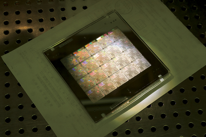
We tend to discuss leading-edge nodes and the most advanced chips made using them, but there are thousands of chip designs developed years ago that are made using what are now mature process technologies that are still widely employed by the industry. On the execution side of matters, those chips still do their jobs as perfectly as the day the first chip was fabbed which is why product manufacturers keep building more and more using them. But on the manufacturing side of matters there's a hard bottleneck to further growth: all of the capacity for old nodes that will ever be built has been built – and they won't be building any more. As a result, TSMC has recently begun strongly encouraging its customers on its oldest (and least dense) nodes to migrate some of their mature designs to its 28 nm-class process technologies.
Nowadays TSMC earns around 25% of its revenue by making hundreds of millions of chips using 40 nm and larger nodes. For other foundries, the share of revenue earned on mature process technologies is higher: UMC gets 80% of its revenue on 40 nm higher nodes, whereas 81.4% of SMIC's revenue come from outdated processes. Mature nodes are cheap, have high yields, and offer sufficient performance for simplistic devices like power management ICs (PMICs). But the cheap wafer prices for these nodes comes from the fact that they were once, long ago, leading-edge nodes themselves, and that their construction costs were paid off by the high prices that a cutting-edge process can fetch. Which is to say that there isn't the profitability (or even the equipment) to build new capacity for such old nodes.
This is why TSMC's plan to expand production capacity for mature and specialized nodes by 50% is focused on 28nm-capable fabs. As the final (viable) generation of TSMC's classic, pre-FinFET manufacturing processes, 28nm is being positioned as the new sweet spot for producing simple, low-cost chips. And, in an effort to consolidate production of these chips around fewer and more widely available/expandable production lines, TSMC would like to get customers using old nodes on to the 28nm generation.
"We are not currently [expanding capacity for] the 40 nm node" said Kevin Zhang, senior vice president of business development at TSMC. "You build a fab, fab will not come online [until] two year or three years from now. So, you really need to think about where the future product is going, not where the product is today."
While TSMC's 28nm nodes are still subject to the same general cost trends as chip fabs on the whole – in that they're more complex and expensive on a per-wafer basis than even older nodes – TSMC is looking to convert customers over to 28nm by balancing that out against the much greater number of chips per wafer the smaller node affords. Therefore, while companies will have to pay more, they also stand to to get more in terms of total chips. And none of this takes into account potential ancillary benefits of a newer node, such as reduced power consumption and potentially greater clockspeed (performance) headroom.
"So, lots of customers' product today is at, let's say 40 nm or even older, 65 nm," said Zhang. They are moving to lower advance nodes. 20/28 nm is going to be a very important node to support future specialty. […] We are working with customer to accelerate [their transition]. […] I think the customer going to get a benefit, economic benefit, scaling benefit, you have a better power consumption. but they've already got a chip that works. Why? Oh, then you could say why we do advanced technology. Yeah. Yeah. I mean, it's, uh, find just the nature of the summit is you go to a next node, you get a better performance and better power and overall you get a system level benefit."
In addition to multiple 28nm nodes designed for various client applications, TSMC is expanding its lineup of specialty 28nm and 22nm (22ULP, 22ULL) process technologies to address a variety of chip types that currently rely on various outdated technologies. As with the overall shift to 28nm, TSMC is looking to corral customers into using the newer, higher density process nodes. And, if not 28nm/22nm, then customers also have the option of transitioning into even more capable FinFET-based nodes, which are part of TSMC's N16/N12 family (e.g., N12e for IoT).


19 Comments
View All Comments
thestryker - Wednesday, June 29, 2022 - link
There will also never be any expansion in capacity at the higher nodes. If there are currently backlogs on a node they will never get better unless people switch to newer nodes.DanNeely - Tuesday, July 5, 2022 - link
Never say never. the 50% increase in a node as old as 28nm is nearly unprecedented but being driven by surging demand for ICs that don't need anything close to leading edge fabbing; and IIRC other foundries are also increasing legacy capacity as a result of it too.And while TSMC might not do so, there are other companies who only do larger and simpler processes. If TSMC eventually does wind down some legacy processes entirely, companies who can't compete on the high end can be expected to pick up the demand from customers with products that can't physically or economically be moved to smaller nodes.
name99 - Wednesday, June 29, 2022 - link
You don't have to move EVERYONE over, you just have to move the low-lying fruit over.If you have serious difficulty in moving stay on 40nm, but if you can move, so so, and free up space for the laggards.
And if you are a laggard, well, what's your long term plan? To be selling year 2000 tech in 2040? Seriously???
ULTIMATELY this will prove to be a story we have seen time and again.
Some companies prefer to remain fat and lazy, sticking with what they know how to do. And that will be OK for a *few* more years.
Meanwhile other companies can see which way the wind is blowing, will design from scratch to match new reality, will get the new regulatory approval, and will replace the dinosaurs.
Just ask Intuit or Blackberry how well it plays out to ignore where the puck is headed...
SkipPerk - Wednesday, June 29, 2022 - link
This might be true in “tech” fields, but in other sectors continuity is prized, especially if a new chip requires new regulatory approval. That said, too many companies make these transitions needlessly complex by updating everything (there is no need for software changes when shrinking to 28h).Many products do not require cutting edge, and in many fields the decline in product quality over the years often leads to older products being more valuable that the latest new release. Sometimes a chip simply needs to meet the spec, and nothing more. This is increasingly true for software as well (and why Linus is so much safer to use than anything Windows given how tricky getting an old version of windows can be)
FunBunny2 - Thursday, August 11, 2022 - link
To be selling year 2000 tech in 2040? Seriously???battery powered autos are more than a 100 years old. same for gas and diesel. until the supply of Mr. Fusion power plants picks up, we'll be using them for another 100 years.
Duncan Macdonald - Wednesday, June 29, 2022 - link
Small devices (eg power management ICs) get no benefit from being on a smaller node and many devices CANNOT be made on a smaller node due to the required voltages. (When you have insulator thicknesses measured in a few atoms there is a hard limit on the maximum usable voltage.)evanh - Wednesday, June 29, 2022 - link
Now's also a good time for said customers to be quietly raising their own prices to cover such a transition.HarryVoyager - Saturday, July 2, 2022 - link
One other factor is node rot. I've notice old node seem to eventually start to have yield problems. I recall one ancient chip we used that the manufacturer simply decided to stop making because their yield had taken a nose dive.The chip itself was stupidly cheap, and the replacement was stupidly cheap, but the ripple effects were a massive pain. Had different voltages and different physical layout, so we had to respin a PCB and write new firmware to deal with it. Ended up stupid expensive. Would have cheerfully taken a last time buy at way more than the original price, but the process just futzed out, so redesign ho we had to go.
I suspect consolating on a single node means they can have some additional staff focused on making sure that mode keeps working, as opposed to spreading their crew out over a dozen or so similar but different processes.
TomWomack - Saturday, July 9, 2022 - link
Unless TSMC can provide some really quite elaborate level-shifting circuitry in the space that's freed up by moving to a newer node, there's going to be trouble producing a 28nm chip that has the same footprint and voltages as a 65nm one.And I think by 28nm you're using multiple patterning and have really rather tight design rules; you can't just put the 65nm masks into a 28nm stepper and have them projected with really crisp corners.