Everything You Always Wanted to Know About SDRAM (Memory): But Were Afraid to Ask
by Rajinder Gill on August 15, 2010 10:59 PM ESTIt’s coming up on a year since we published our last memory review; possibly the longest hiatus this section of the site has ever seen. To be honest, the reason we’ve refrained from posting much of anything is because things haven’t changed all that much over the last year – barring a necessary shift towards low-voltage oriented ICs (~1.30V to ~1.50V) from the likes of Elpida and PSC. Parts of these types will eventually become the norm as memory controllers based on smaller and smaller process technology, like Intel’s 32nm Gulftown, gain traction in the market.
While voltage requirements have changed for the better, factors relating to important memory timings like CL and tRCD haven’t seen an improvement; we’re almost at the same point we were a year ago. Back then Elpida provided a glimpse of promise with their Hyper-series of ICs. The Hyper part was capable of high-speed, low-latency operation in tandem. Unfortunately, due to problems with long-term reliability, Hyper is now defunct. Corsair and perhaps Mushkin still have enough stock to sell for a while, but once it's gone, that’s it.
The superseding Elpida BBSE variant ICs and a spread of chips from PSC now dominate the memory scene, ranging from mainstream DDR3-1333 speeds all the way to insanely-rated premium DDR3-2500 kits. Some of these parts are capable of keeping up with Hyper when it comes to CL, but do so by adding a few nanoseconds of random access latency due to a looser tRCD. Given that read and write access operations make up a significant portion of memory power consumption, this step backwards in performance may be a requisite factor for reliability – perhaps something was found by Elpida during the production lifetime of Hyper ICs that prompted a re-examination, leading to a more conservative recipe for data transfer/retrieval.
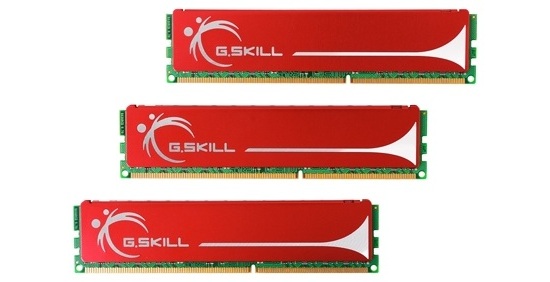
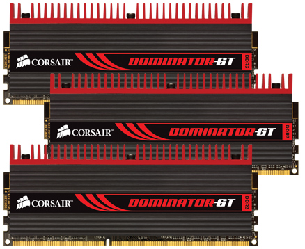
Today’s memory section comeback was fuelled by the arrival of a number of mainstream memory kits at our test labs – many of the kits we were using for motherboard reviews are no longer for sale so we needed to update our inventory of modules anyway. Corsair, Crucial and GSkill kindly sent memory from their mainstream line-ups. The original intent was to look at a few of those kits.
However, during the course of testing these kits, our focus shifted from writing a memory review (showing the same old boring graphs) to compiling something far more meaningful: a guide to memory optimization and addressing, including a detailed look at important memory timings, and an accounting of some of Intel’s lesser-known memory controller features. As such, this article should make a very compelling read for those of you interested in learning more about some of the design and engineering that goes into making memory work, and how a little understanding can go a long way when looking for creative ways to improve memory performance…


46 Comments
View All Comments
ekoostik - Tuesday, August 17, 2010 - link
Great article. Going to take me a few more reads. One question - why no mention of Command Rate (and I double checked the Memory Scaling on Core i7 article, absent there too)? CR is often included in RAM specs, e.g. 9-9-9-24-2T, but never fully discussed if mentioned at all. Is it just not important anymore?Muhammed - Tuesday, August 17, 2010 - link
Ok I managed to royally confuse my self !What I know is that DDR3 operates at 1/8 the rated frequency , that means in case of DDR3 @800MHz , the internal memory operations are actually running at 100MHz , but the memory is able to fetch 8-words every clock cycle .
So 100MHz X (8 words ) = 800 Word per second as data rate , then the manufacturer misleadingly label the RAM module as a 800MHz part .
so the real benefit of DDR3 over DDR or DDR2 comes not from increased operating frequency , but from higher bandwidth .
To stress that fact , I mention DDR2 @800MHz , it operates at 200Mhz (internal clock) , however it only fetches 4-words every clock cycle , (200X4 = 800 Words).
When DDR3 operates at 200MHz (internal operations) like DDR2 , it fetches double the data , effectively managing 1600 words per second .
NOW , in your article .. you mention the base clock (I/o Bus) and you mention the double data rate , I know the I/O Bus clock is always 2 or 4 times the internal clock , so DDR3 @ 100MHz , has a 400MHz I/O bus .. but I couldn't understand the I/O bus function and it's relation in data transmission and data rate .
I am missing something here , could you enlighten me ?
Edison5do - Tuesday, August 17, 2010 - link
I Really was Affraid..!!Edison5do - Tuesday, August 17, 2010 - link
Technical Reading !!! LOve Thishasherr - Wednesday, August 18, 2010 - link
Great article. But what i dont get is how the hell motherboard knows all those timings? In SPDs there are like N timings described, isnt there really more? At least in bios settings i see more.Another thing. I buy Kingston 1800 MT/s module, with SPDs up to 1333 MTs. I overclock and make it run @ rated 1800mt/s speed. All timings are on auto. How the hell mobo/bios guess all of them :)?
ClagMaster - Wednesday, August 18, 2010 - link
Afraid to Ask ?After perusing through this I find myself afraid to read.
Comprehensive article for a novice EE
just4U - Wednesday, August 18, 2010 - link
Great article and ..." ....should be to focus development on reducing absolute minimum latency requirements for timings such as CAS and tRCD, rather than chasing.."
I hope the memory makers and shakers out there read that!!
lyeoh - Saturday, August 21, 2010 - link
The mistake counter bit counts seem OK to me. In what way are they wrong?There are 9 MSB (most significant bits) in the table.
Yes there are 13 bits in the counter, but the 9 bits in the table only refer to the 9 "top bits" of those 13 bits.
For example, if I have an 8 bit counter but 4 bits in some table only refer to the 4 most significant bits, then that means that you'd only see all zeroes in those 4 bits when the counter has values from 0 to 15 (0x0 to 0xF). When the counter has values from 240 to 255 (0xF0 to 0xFF), you'd see all ones in those 4 bits.
As for the description, I don't know the details of how the stuff works, so I don't know whether it's wrong or not.
dia - Saturday, August 21, 2010 - link
Read the explanation here:http://download.intel.com/design/processor/datasht...
Page 79.
To quote:
"MISTAKECOUNTER.
This field is the upper 8 MSBs of a 12-bit counter. This counter adapts the
interval between assertions of the page close flag. For a less aggressive page
close, the length of the count interval is increased and vice versa for a more
aggressive page close policy."
Now look at the left hand column, it shows 8:0. That's 9 bits! It's a 13 bit counter.
If it were a 12 bit counter the maximum permissible selection value would be 4095 and not 8191.
datasegment - Saturday, August 21, 2010 - link
Quick fyi - 8k is not 8196, it is 8192 :)