Toshiba Brings Through-Silicon Vias to NAND Flash
by Billy Tallis on August 12, 2015 8:01 AM EST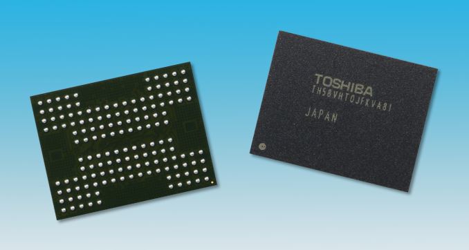
At Flash Memory Summit this week, Toshiba is showing off a NAND flash device packaged using through-silicon vias rather than traditional wire-bonded connections.
The NAND flash currently on the market is typically produced in the form of a die with a capacity like 128Gb (16GB). The popular SSD form factors don't have enough surface area to fit dozens of those chips, and SSD controllers don't have the pin count to connect to that many independently, so several chips are stacked in a single postage-stamp sized package. The traditional way of connecting the individual dies in a stack is to use the same technique as for a single-die package: bonding a thin gold wire between the edge of the die and the package substrate or external pins. The downsides are that it requires a lot of wires and the edges of the dies in the stack need to be exposed somehow, either by staggering them or by putting a spacer between each layer.
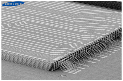
An alternative packaging method is to design the dies to participate in the stacking, by including electrical conductors that penetrate the entire thickness of the silicon die so that they can make contact with the dies above and below it in the stack, essentially tunneling right through each die. These through-silicon vias (TSVs) can then form a shared bus to carry signals from any of the dies in the stack out to the last die, which is the only one with the external connections.
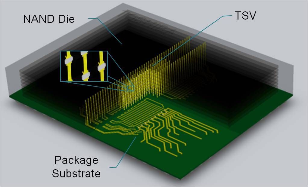
Chip stacking using TSVs requires the dies to be aligned and stacked without spacers, which makes the whole stack a bit more compact. Since TSVs can be placed anywhere on the chip rather than just at the edge, it's easy to implement a wide data bus and communication within the stack can be very fast or low-power due to the short distances involved. These advantages have been very attractive for packaging DRAM, most notably in the form of the HBM stacks used by AMD's R9 Fury and R9 Nano video cards.
Toshiba's demonstration is a 16-high stack of 128Gb dies in a BGA-152 package measuring 14mm by 18mm and 1.9mm thick, and an 8-high stack that's 1.35mm thick. Those numbers are all typical even for wire-bonded stacks. The speed (1Gb/s) and operating voltages (1.2V for I/O and 1.8V core) are what we would expect from a next-generation NAND interface, but the claimed 50% power reduction is a very nice improvement for a change that leaves the flash memory cells themselves unmodified.
Toshiba hasn't said whether the dies being stacked are their current 15nm planar NAND or their forthcoming 3D NAND, nor have they said when modules using TSVs will be hitting the market. The most compelling applications would be to use TSVs to stack flash atop a controller chip in an eMMC product or atop an SoC, but the power savings would be appreciated almost everywhere. If the use of TSVs allows economically stacking more than 16 dies, it could enable a dramatic increase in the density of SSDs.


18 Comments
View All Comments
T1beriu - Thursday, August 13, 2015 - link
He's not talking about PR drops. He's complaining about the massive ad banners that started to cover the site.bill.rookard - Wednesday, August 12, 2015 - link
Be a little proactive. Adblock Plus (assuming a Firefox user) does a wonderful job of eliminating all that garbage (well, ok, 99.9%).Impulses - Thursday, August 13, 2015 - link
Hadn't even noticed, ads haven't changed on mobile... Still one per page at the bottom of the page.lilmoe - Wednesday, August 12, 2015 - link
I wonder what kind of impact this would have on performance if these were used in a traditional SSD layout. To what extent is parallelism affected? How does the speed of those stacked dies compare against traditional planar NAND? (1Gb/s vs ???)Billy Tallis - Wednesday, August 12, 2015 - link
ONFI 4.0 specifies 800Mb/s, so the speed boost is an incremental improvement, not revolutionary. The reason is that it's still a BGA-152 package providing a 16-bit interface. If the NAND were stacked onto an interposer along with the controller (ie. how AMD uses HBM), then a really wide interface would be practical.lilmoe - Wednesday, August 12, 2015 - link
Which means that even the 50% power reduction isn't as revolutionary either since the overall efficiency of more dies in parallel might be the same or even higher...lilmoe - Wednesday, August 12, 2015 - link
They might not replace traditional SSDs in terms of speed, latency and efficiency, but I could see the real potential of these replacing HHDs in terms of capacity and cost. We might even see hybrid solutions too.triadone - Thursday, August 13, 2015 - link
Isn't this what spurred the terminators?