The Intel Skylake Mobile and Desktop Launch, with Architecture Analysis
by Ian Cutress on September 1, 2015 11:05 PM EST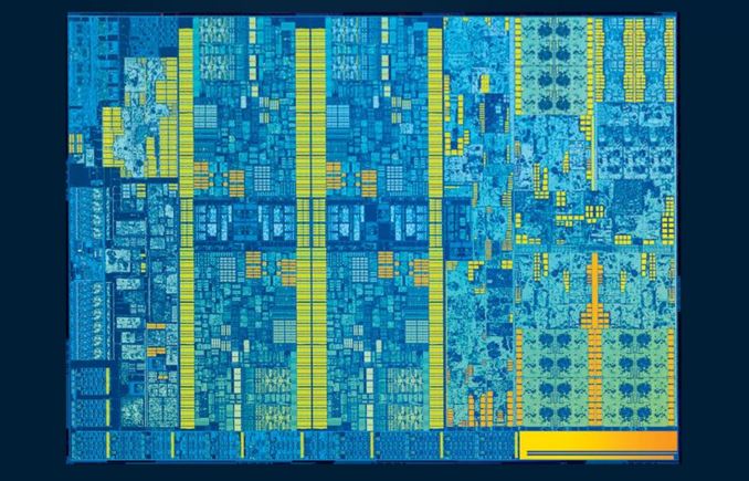
Intel’s 6th Generation of its Core product line, Skylake, is officially launching today. We previously saw the performance of the two high end Skylake-K 91W processors, but that was limited in detail as well as product. So it is today that Intel lifts the lid on the other parts from 4.5 W in mobile through Core M, to 15W/28W in Skylake-K, 45W in Skylake-H and then the 35W/65W mêlée of socketed Skylake-S parts. For today's formal launch we will be taking a look at the underlying Skylake architecture, which was unveiled by Intel at their recent Intel Developer Forum this August.
The (Abridged) March to Skylake and Beyond
For Intel, the Skylake platform is their second swing at processors built on the 14nm process node, following the launch of Broadwell late in 2014. The main difference from Broadwell is that Skylake is marked as a substantial change in the underlying silicon, introducing new features and design paradigms to adjust to the requirements that now face computing platforms in 2015-2016, even though the design of Skylake started back in 2012.
| Intel's Tick-Tock Cadence | |||||
| Microarchitecture | Process Node | Tick or Tock | Release Year | ||
| Conroe/Merom | 65nm | Tock | 2006 | ||
| Penryn | 45nm | Tick | 2007 | ||
| Nehalem | 45nm | Tock | 2008 | ||
| Westmere | 32nm | Tick | 2010 | ||
| Sandy Bridge | 32nm | Tock | 2011 | ||
| Ivy Bridge | 22nm | Tick | 2012 | ||
| Haswell | 22nm | Tock | 2013 | ||
| Broadwell | 14nm | Tick | 2014 | ||
| Skylake | 14nm | Tock | 2015 | ||
| Kaby Lake (link)? | 14nm | Tock | 2016 ? | ||
Intel’s strategy since 2008 is one of tick-tock, alternating between reductions in process node at the point of manufacture (which reduces die area, leakage and power consumption but keeps the layout similar) and upgrades in processor architecture (improve performance, efficiency) as shown above. Skylake is the latter, which will be explained in the next few pages.
The Launch Today
Typically a complete product stack of processors for Intel runs the gamut from low power to high power, including i7, i5, i3, Pentium, Celeron and Xeon. This also applies on the integrated graphics side, from base HD designs to GT1, GT2, GT3/e and beyond. In a departure from their more recent launches, Intel is launching nearly their entire Skylake product stack today in one go, although there are some notable exceptions.
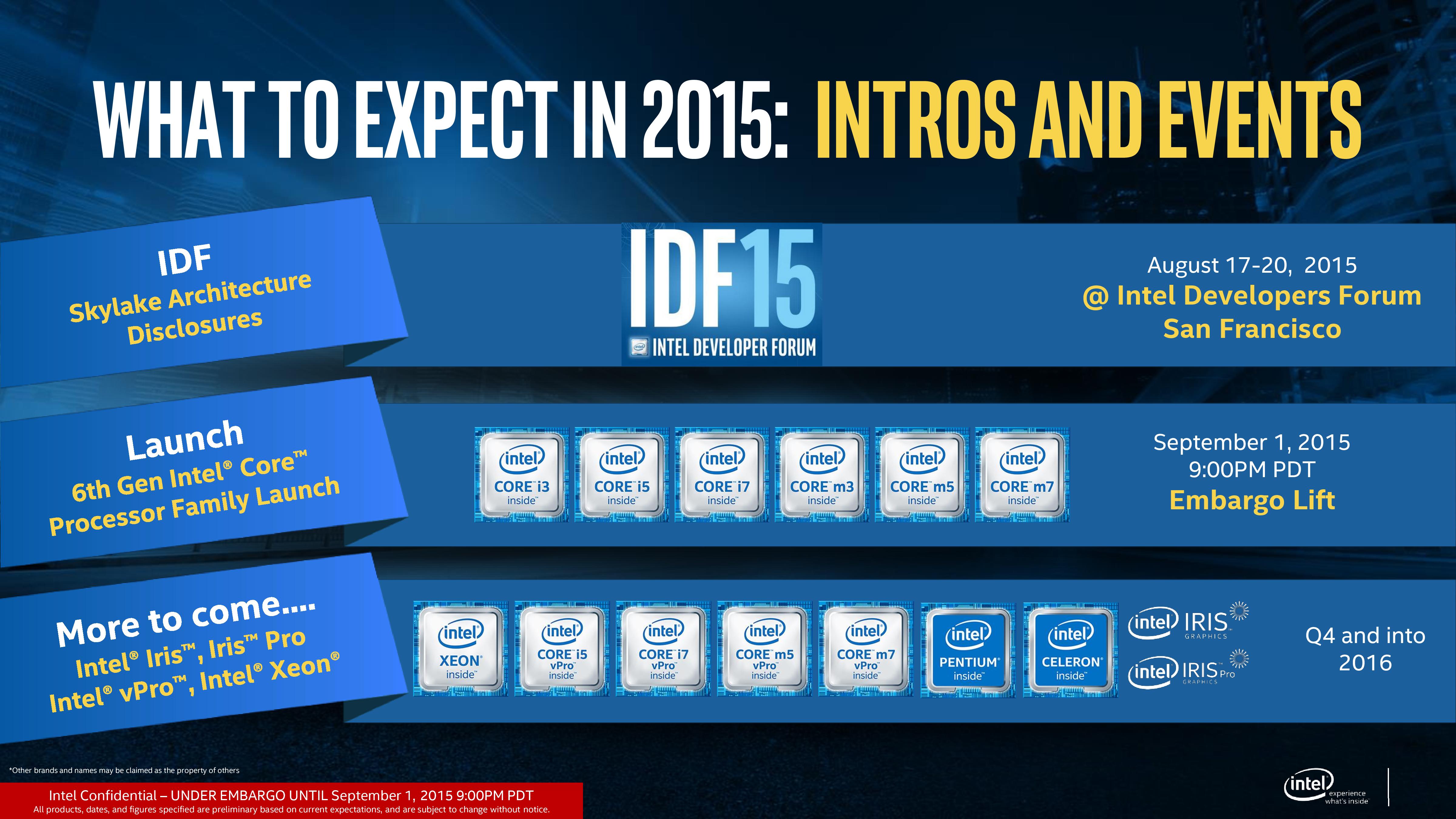
All of the Core M processors are launching today, as are the i3/i5/i7 models and two new Xeon mobile processors. From a power perspective this means Intel is releasing everything from the 4.5W ultra-mobile Core M through the large 65W desktop models, along with the previously released 91W desktop SKUs. What parts that are not launching today are the Pentium/Celeron processors, the E3 v5 desktop Xeons, and the vPro enabled processors. Put another way, Intel is launching most of their 2+2 and 4+2 SKUs today, with the exception of budget SKUs and some of Intel's specialized IT/workstation SKUs.
Meanwhile for SKUs with Intel's high end Iris and Iris Pro integrated graphics – the 2+3 and 4+4 die configurations – Intel will also be launching these at a later time. For the Iris configurations Intel is staying relatively vague for the moment, telling the press that we should expect to see those parts launch in Q4'15/Q1'16. That being said, the annual Consumer Electronics Expo in Las Vegas is being held in the first week of January, so we imagine we should see some movement there, if not before.
Today's launch will also come with a small change in how Intel brands their Core M lineup of processors. With the Broadwell generation Intel used a mix of 4 and 5 character product identifiers, e.g. Core M 5Y10a. However for the Skylake generation the Core M naming scheme is being altered to better align with Intel's existing mainstream Core i-series parts and hopefully cut down on some of the confusion in the process. Thus we now have Core m3, m5 and m7 to complement the i3, i5 and i7 already used on Intel's more powerful processors. This will be represented by both Intel and the OEMs when it comes down to device design to afford greater differentiation in the Core M product line.
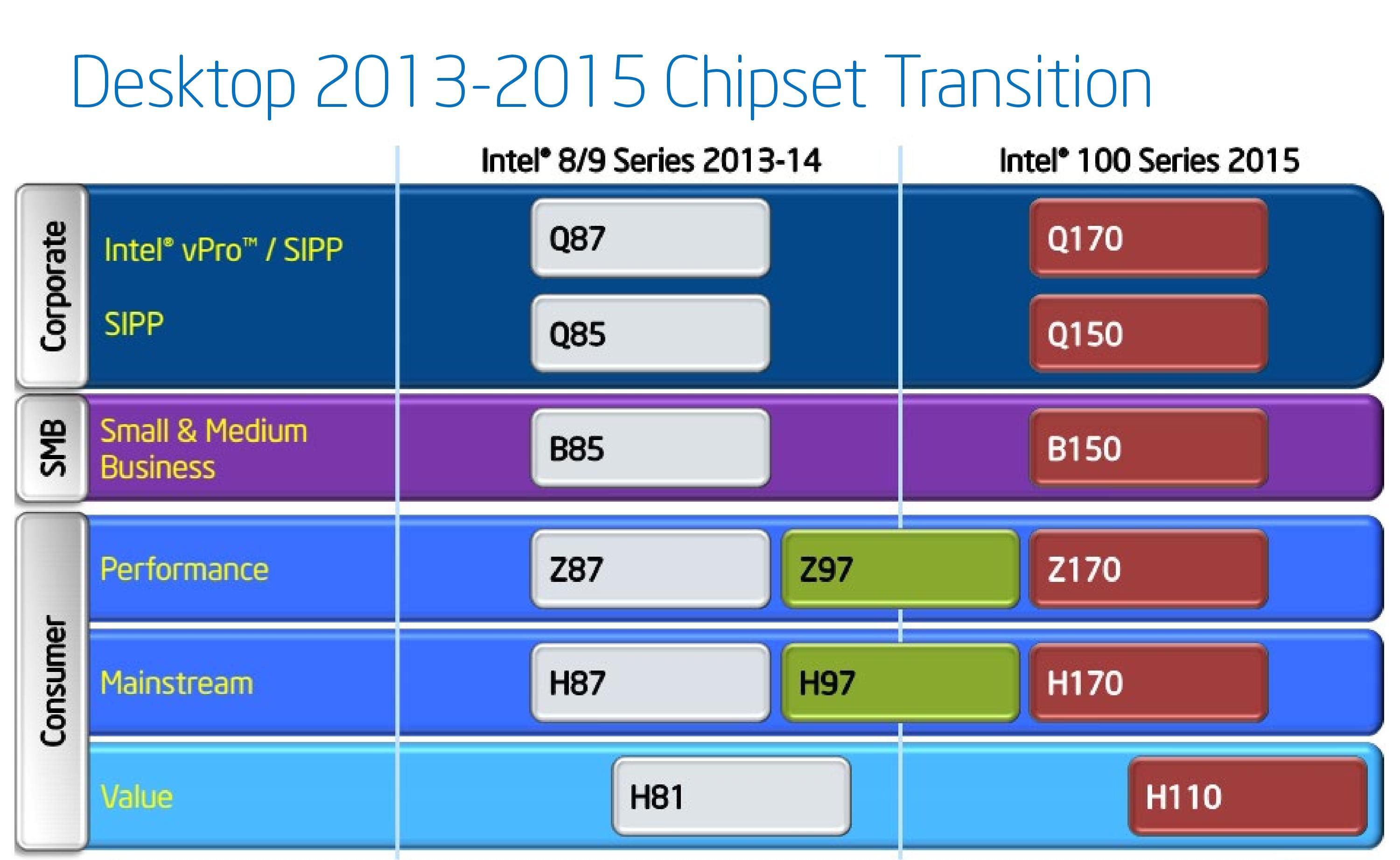
Launching secondary to the processors, and perhaps not promoted as much, are the new Intel 100-series chipsets. Specifically, there will be desktop motherboard manufacturers announcing motherboards based on H170, B150, H110 and Q170 today, although which of these will be available when (for both desktop and other use) is not known. We have been told that the business oriented chipsets (B150/Q1x0) will have information available today but won’t necessarily ‘launch’. We have information on these later in the review
As a result of all these processor and chipset families coming to market at once, as well as linking up the launch to the Internationale Funkausstellung Berlin (IFA) show held in Berlin, Germany, Intel’s launch is going to be joined by a number of OEMs releasing devices as well. Over the course of IFA this week (we have Andrei on site), we expect Lenovo, ASUS, Dell, HP and others to either announce or release their devices based around Skylake. We covered a number of devices back at Computex in June advertised as having ‘6th Generation’ processors, such as MSI’s AIOs and notebooks, so these might also start to see the light of day with regards to specifications, pricing, and everything else.

A Skylake wafer shown at IDF 2015
The Parts
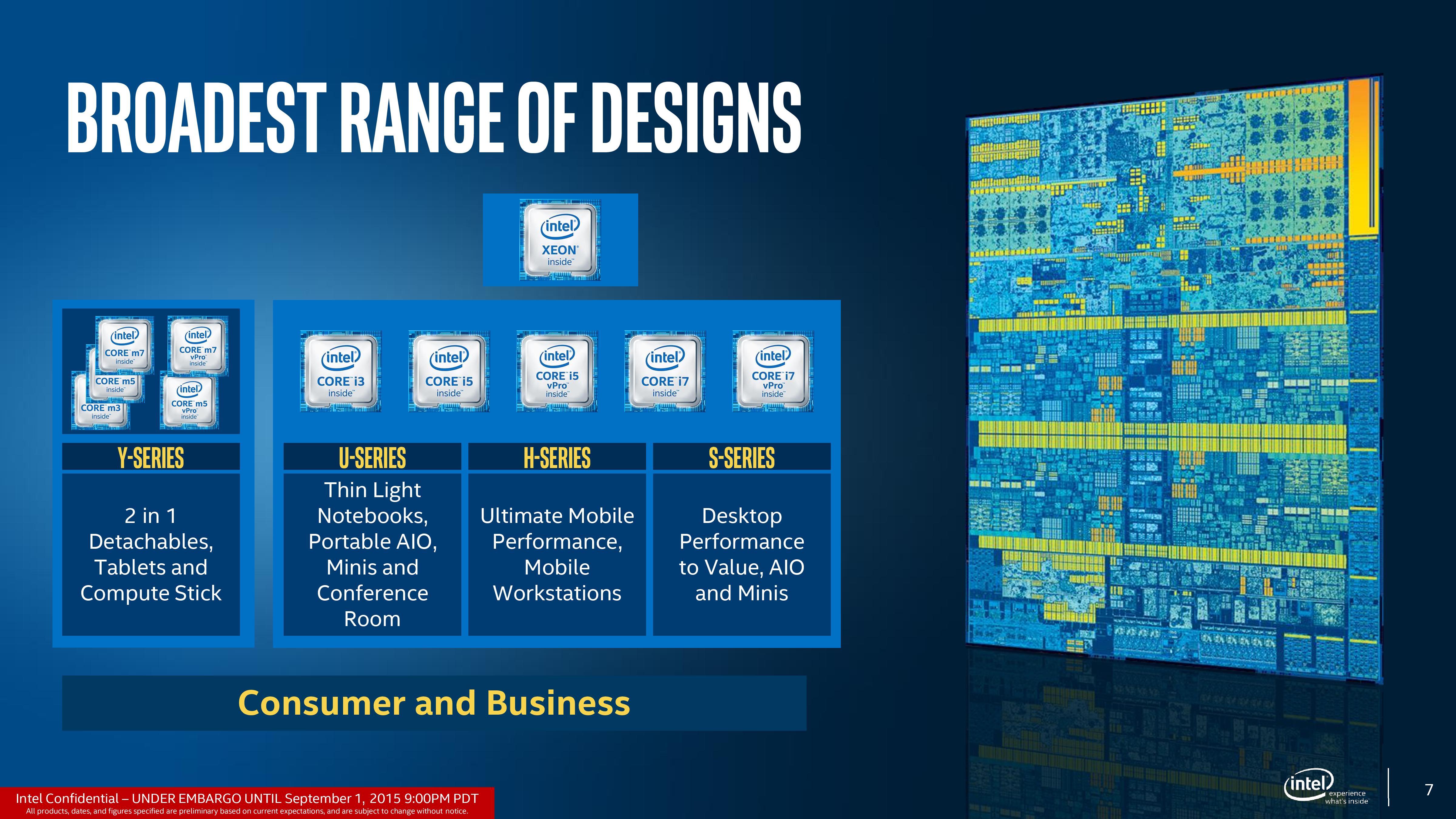
To cut to the chase, the processor base designs come from five dies in four different packages. The terms ‘Skylake-Y’, ‘Skylake-U’, ‘Skylake-H’ and ‘Skylake-S’ are used as easy referrals and loosely define the power consumption and end product that these go in, but at the end of the day the YUHS designation can specifically segregate the size of the package (the PCB on which the die and other silicon sits). The YUHS processors all feature the same underlying cores, the same underlying graphics units, but differ in orientation and frequency. The best way to refer to these arrangements is by the die orientation, such as 2+2 or 4+4e. This designation means the number of cores (2 or 4) and the level of graphics (2 or 3e or 4e).

Core M designs, which fall under Skylake’s Y-series, will be available in a 2+2 configuration only which is similar to the Broadwell offerings. This allows Intel to keep around the 4.5W margins, and as with Broadwell, many of these processors will have a low base frequency and a high turbo mode to take advantage of burst performance. However, if you read our piece on the problems of OEM design on Broadwell’s Core M, it can depend highly on the device manufacturer as to the end performance you might receive. Intel states that for Skylake, this becomes less of an issue, and we cover this later in this article. By virtue of the desire to reduce the number of packages in these devices, the chipset/IO is integrated on the package. Also to note, DRAM support for Skylake-Y will be limited to LPDDR3/DDR3L, and will not include DDR4 support like the others. We suspect this is either for power reasons or because DDR4 needs more pins, but when DDR4L comes to play we should see future Core M platforms migrate in that direction.
Skylake-U also follows a similar path to previous Intel generations, being available in 15W and 28W versions. What is new comes down to the configurations – 2+2 as expected but also 2+3e models will be available later in the year. The extra ‘e’ means that these versions will also include Intel’s eDRAM solution which we have seen to be significantly useful when it comes to graphics performance. In previous eDRAM designs, this was only in available in 128MB variants, but for Skylake-U we will start to see 64MB versions. These will also be on package, similar to the chipset/IO, resulting in a 42x24mm package arrangement.
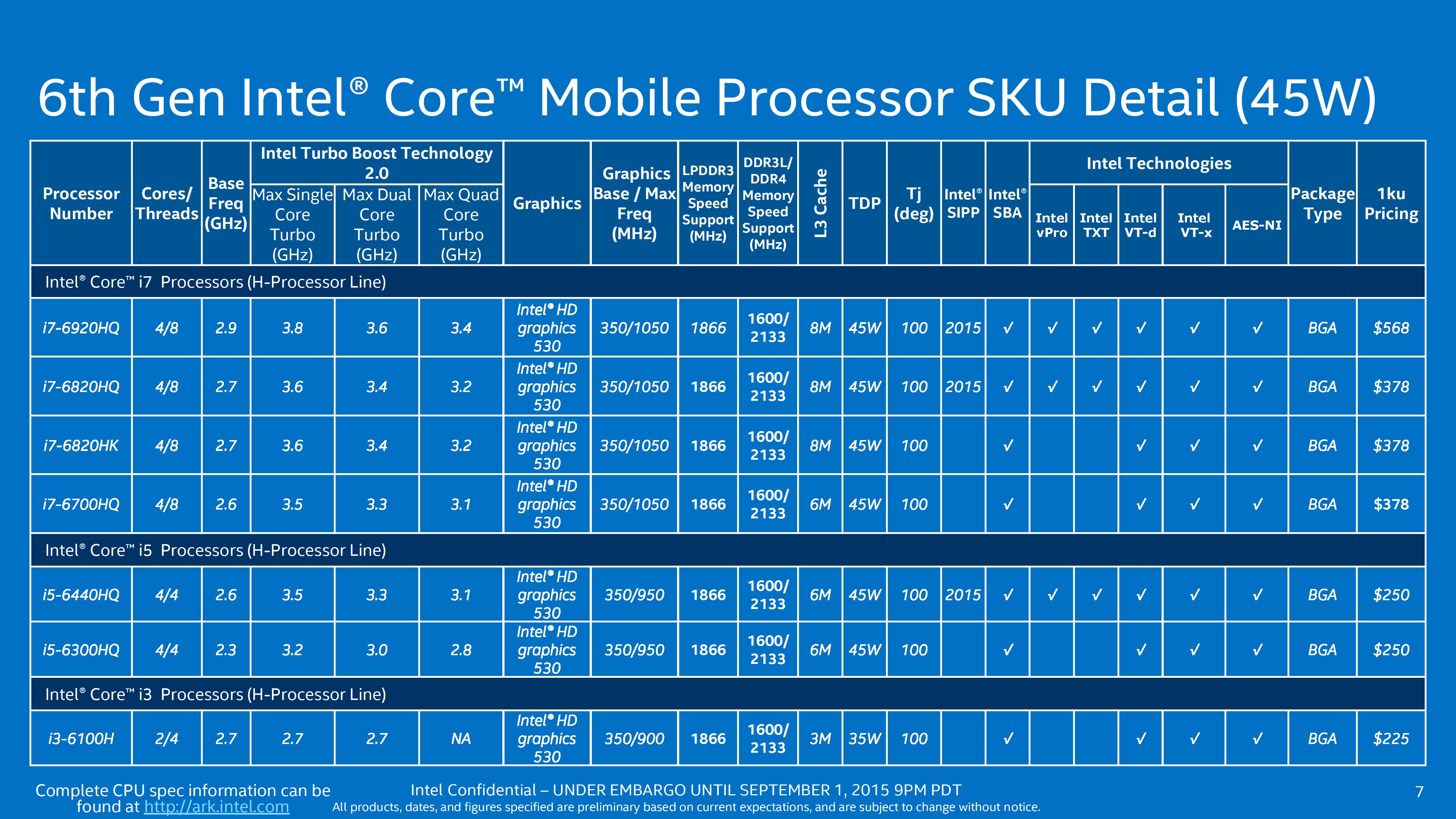
The H processor family, such as Skylake-H, is typically found in high end notebooks or specific market devices such as all-in-ones where the ability to deal with the extra TDP (45W) is easier. Historically the H processor family is BGA only, meaning it can only be found in products soldered directly to the motherboard. With Broadwell-H, Intel released a handful of socketable processors for desktop/upgradeable AIO designs, but with the information given above this might not happen for Skylake. Nevertheless, Skylake-H will feature 45W parts with 4+2 and 4+4e configurations, the latter having 128MB of eDRAM. Also similarly to previous H designs, the chipset is external to the processor package.
Skylake-S represents everything desktop, including the K processors. Some users will be disappointed that despite the move to 14nm, Intel is still retaining the 2+2 and 4+2 configurations with no six-core configuration on the horizon without moving up to the high-end desktop (HEDT) platform (and back two generations in core architecture). Nevertheless, alongside the two 91W overclocking ‘Skylake-K’ parts we have seen already, Intel will launch the regular 65W parts (e.g. i7-6700, i5-6600, i3-6100) and lower power ‘Skylake-T’ 45W (i7-6700T, i5-6600T, i3-6100T) parts as well. These will all have GT2 graphics, varying in frequency, as well as varying in cache sizes and some feature sets. We go more into detail over the next few pages.


We will go over each of the product markets in turn through this review, but the gallery above showcases the 48 different processors that Intel is prepared to announce at this point. This includes Pentium information as well as a few GT3e products (HD Graphics 550, 48 EUs with 64MB eDRAM) that will be released over the next two quarters.
A Small Note on Die Size and Transistor Counts
In a change to Intel’s previous strategy on core design disclosure, we will no longer be receiving information relating to die size and transistor counts as they are no longer considered (by Intel) to be relevant to the end-user experience. This data in the past might have also given Intel's compeititors more information in the public domain than ultimately they would have wanted. But as you might imagine, at AnandTech we want this information – die size allows us to indicate metrics towards dies per wafer and the capable throughput of a fab producing Intel processors. Transistor count is a little more esoteric, but it can indicate where effort, die area and resources are being geared. In the past we have noted how proportionally more die area and transistors are being partitioned in favor of graphics, and changes in that perspective can indicate the market directions that Intel deems as important.
Obtaining die size area is easier than transistor count, as all that needs to be done is to pop off a heatspreader and bring out the calipers (then assume that there’s no frivolous extra silicon, which seems counterintuitive as die area is proportional to dies per wafer and thus potential revenue). With transistor count, it was not clear if Intel would be providing at a minimum a set of false-color die shots with regions marked, meaning that if this is not the case then when other analysts are able to do an extensive SEM analysis, we will get some information at least.

But for now, this is what we know:
| CPU Specification Comparison | |||||
| CPU | Process Node |
Cores | GPU | Transistor Count (Schematic) |
Die Size |
| Intel Skylake-K 4+2 | 14nm | 4 | GT2 | ? | 122.4 mm2 |
| Intel Skylake-Y 2+2 | 14nm | 2 | GT2 | ? | 98.5mm2 |
| Intel Broadwell-H 4+3e | 14nm | 4 | GT3e | ? | ? |
| Intel Haswell-E 8C | 22nm | 8 | - | 2.6 B | 356 mm2 |
| Intel Haswell-S 4+2 | 22nm | 4 | GT2 | 1.4 B | 177 mm2 |
| Intel Haswell ULT 2+3 | 22nm | 2 | GT3 | 1.3 B | 181 mm2 |
| Intel Ivy Bridge-E 6C | 22nm | 6 | - | 1.86 B | 257 mm2 |
| Intel Ivy Bridge 4+2 | 22nm | 4 | GT2 | 1.2 B | 160 mm2 |
| Intel Sandy Bridge-E 6C | 32nm | 6 | - | 2.27 B | 435 mm2 |
| Intel Sandy Bridge 4+2 | 32nm | 4 | GT2 | 995 M | 216 mm2 |
| Intel Lynnfield 4C | 45nm | 4 | - | 774 M | 296 mm2 |
| AMD Trinity 4C | 32nm | 4 | 7660D | 1.303 B | 246 mm2 |
| AMD Vishera 8C | 32nm | 8 | - | 1.2 B | 315 mm2 |
This is taken from our Skylake-K package analysis of the 4+2 arrangement.


173 Comments
View All Comments
Xenonite - Thursday, September 3, 2015 - link
Actually, it seems that power consumption is the only thing that matters to consumers, even on the desktop.All this talk about AMD's lack of competition being the reason why we aren't seeing meaningful generational performance improvements is just that: talk.
The real thing that hampers performance progress is consumers' plain refusal to upgrade for performance reasons (even a doubling in performance is not economically viable to produce since no one, except for me it seems, will buy it).
Consumers only buy the lowest power system that they can afford. It has nothing to do with AMD.
Even if AMD released a CPU that is 4x faster than piledriver, it wouldn't change Intel's priority (nor would it help AMD's sales...).
IUU - Wednesday, September 2, 2015 - link
Sorry for my tone , but "I'm failing to see", how transistor count don't mean more to consumers than to anyone else.So, after 10 years of blissful carelessness(because duuude it's user experience dat matters, ugh..),
you will have everyone deceiving you on what they offer on the price point they offer. Very convenient, especially if they are not able to sustain an exponential increase in performance and passing to the next paradigm to achieve it.
Because untill very recently we have been seeing mostly healthy practices, despite the fact that you could always meet people pointing to big or small sins.
Big example, What's the need of an igp on a processor that consumes 90 watts, especially a gpu that is tragically subpar? To hide the fact they have nothing more to offer to the consumer, cpu dependent, at 90 watts(at the current market situation) and have an excuse for charging more on a
theoretically higher consuming and "higher performing" cpu?
Because, what bugs me is what if 6700k lacked the igp? Would it perform better without a useless igp dragging it down? I really don't know, but I feel it wouldn't.
Regarding the mobile solutions and the money and energy limited devices, the igp could really prove to be useful to a lot of people, without overloading their device with a clunky, lowly, discrete gpu.
xenol - Wednesday, September 2, 2015 - link
If the 6700K lacked the iGPU with no other modifications, it would perform exactly the same.MrSpadge - Wednesday, September 2, 2015 - link
Yes, it would perform exaclty the same (if the iGPU is not used, otherwise it needs memory bandwidth). But the chip would run hotter since it would be a lot smaller. Si is not the best thermal conductor, but the presence of the iGPU spreads the other heat producers a bit.xenol - Wednesday, September 2, 2015 - link
I don't think that's how thermals in ICs work...MrSpadge - Wednesday, September 2, 2015 - link
Thermodynamics "work" and don't care if they're being applied to an IC or a metal brick. Silicon is a far better heat conductor than air, so even if the GPU is not used, it will transfer some of the heat from the CPU + Uncore to the heat spreader.My comment was a bit stupid, though, in the way that given how tightly packed the CPU cores and the uncore are, the GPU spreads none of them further apart from each other. It could have been designed like that, but according to the picture on one of first few pages it's not.
Xenonite - Thursday, September 3, 2015 - link
No, it wouldn't. You could easily spread out the cores by padding them with much more cache and doubling their speculative and parallel execution capabilities. If you up the power available for such out of order execution, the additional die space could easily result in 50% more IPC throughput.MrSpadge - Thursday, September 3, 2015 - link
50% IPC increase? Go ahead and save AMD, then! They've been trying that for years with probably billions of R&D budget (accumulated over the years), yet their FX CPUs with huge L3 don't perform significantly better than the APUs with similar CPU cores and no L3 at all.Xenonite - Thursday, September 3, 2015 - link
Yes, but I specifically mentioned using that extra cache to feed the greater amount of speculative execution units made available by the removal of the iGPU.Sadly, AMD can't use this strategy because Global Foundaries' and TSMC's manufacturing technology cannot fit the same amount of transistors into a given area, as Intel's can.
Furthermore, their yields for large dies are also quite a bit lower and AMD really doesn't have the monetary reserves to produce such a high-risk chip.
Also, the largest fraction of that R&D budget went into developing smaller, cheaper and lower power processors to try and enter the mobile market, while almost all of the rest went into sacrificing single threaded design (such as improving and relying more on out of order execution, branch prediction and speculative execution) to design Bulldozer-like, multi-core CPUs (which sacrifice a large portion of die area, that could have been used to make a low amount of very fast cores, to implement a large number of slow cores).
Lastly, I didn't just refer to L3 cache when I suggested using some of the free space left behind by the removal of the iGPU to increase the amount of cache. The L1 and L2 caches could have been made much larger, with more associativity to further reduce the amount and duration of pipeline stalls, due to not having a data dependancy in the cache.
Also, while it is true that the L3 cache did not make much of a difference in the example you posted, its also equally true that cache performance becomes increasingly important as a CPU's data processing throughput increases.
Modern CPU caches just seem to have stagnated (aside from some bandwidth inprovements every now and then), because our CPU cores haven't seen that much of a performance upgrade since the last time the caches have been improved.
Once a CPU gets the required power and transistor budgets for improved out of order performance, the cache will need to be large enough to hold all the different datasets that a single core is working on at the same time (which is not a form a multi-threading in case you were wondering), while also being fast enough to service all of those units at once, without adversely affecting any one set of calculations.
techguymaxc - Wednesday, September 2, 2015 - link
Your representation of Skylake's CPU/IPC performance is inaccurate and incomplete due to the use of the slowest DDR4 memory available. Given the nature of DDR4 (high bandwidth, high latency), it is an absolute necessity to pair the CPU with high clockspeed memory to mitigate the latency impairment. Other sites have tested with faster memory and seen a much larger difference between Haswell and Skylake. See Hardocp's review, (the gaming section specifically) as well as Techspot's review (page 13, memory speed comparison). Hardocp shows Haswell with 1866 RAM is actually faster than Skylake with 2133 RAM in Unigine Heaven and Bioshock Infinite @ lowest quality settings (to create a CPU bottleneck). I find Techspot's article particularly interesting in that they actually tested both platforms with fast RAM. In synthetic testing (Sandra 2015) Haswell with 2400 DDR3 has more memory bandwidth than Skylake with 2666 DDR4, it is not until you pair Skylake with 3000 DDR4 that it achieves more memory bandwidth than Haswell with 2400 DDR3. You can see here directly the impact that latency has, even on bandwidth and not just overall performance. Furthermore in their testing, Haswell with 2400 RAM vs. Skylake with 3000 RAM shows Haswell being faster in Cinebench R15 multi-threaded test (895 vs. 892). Their 7-zip testing has Haswell leading both Skylake configurations in a memory-bound workload (32MB dictionary) in terms of instructions per second. Finally, in a custom Photoshop workload Haswell's performance is once again sandwiched between the two Skylake configurations.Clearly both Haswell and Skylake benefit from faster memory. In fact, Skylake should ideally be paired with > 3000 DDR4 as there are still scenarios in which it is slower than Haswell with 2400 DDR3 due to latency differences.
Enthusiasts are also far more likely to buy faster memory than the literal slowest memory available for the platform, given the minimal price difference. Right now on Newegg one can purchase a 16GB DDR3 2400 kit (2x8) for $90, a mere $10 more than an 1866 16GB kit. With DDR4 the situation is only slightly worse. The cheapest 16GB (2x8) 2133 DDR4 kit is $110, and 3000 goes for $135. It is also important to note that these kits have the same (primary) timings with a CAS latency of 15.
So now we come to your reasoning for pairing Skylake with such slow RAM, and that of other reviewers, as you are not the only one to have done this. Intel only qualified Skylake with DDR4 up to 2133 MT/s. Why did they do this? To save time and money during the qualification stage leading up to Skylake's release. It is not because Skylake will not work with faster RAM, there isn't an unlocked Skylake chip in existence that is incapable of operating with at least 3000 RAM speed, and some significantly higher. Hardocp was able to test their Skylake sample (with no reports of crashing or errors) with the fastest DDR4 currently available today, 3600 MT/s. I have also heard anecdotally from enthusiasts with multiple samples that DDR4 3400-3600 seems to be the sweet spot for memory performance on Skylake.
In conclusion, your testing method is improperly formed, when considered from the perspective of an enthusiast whose desire is to obtain the most performance from Skylake without over-spending. Now, if you believe your target audience is not in fact the PC enthusiast but instead a wider "mainstream" audience, I think the technical content of your articles easily belies this notion.