GlobalFoundries Teams Up with Singapore University for ReRAM Project
by Anton Shilov on October 28, 2019 11:30 AM EST- Posted in
- Memory
- GlobalFoundries
- ReRAM
- MRAM

GlobalFoundries has announced that the company has teamed up with Singapore’s Nanyang Technological University and the National Research Foundation to develop resistive random access memory (ReRAM). The next-generation memory technology could ultimately pave the way for use as a very fast non-volatile high-capacity embedded cache. The project will take four years and will cost S$120 million ($88 million).
Under the terms of the agreement, the National Research Foundation will provide the necessary funding to Nanyang Technological University, which will spearhead the research. GlobalFoundries will support the project with its in-house manufacturing resources, just like it supports other universities on promising technologies, the company says.
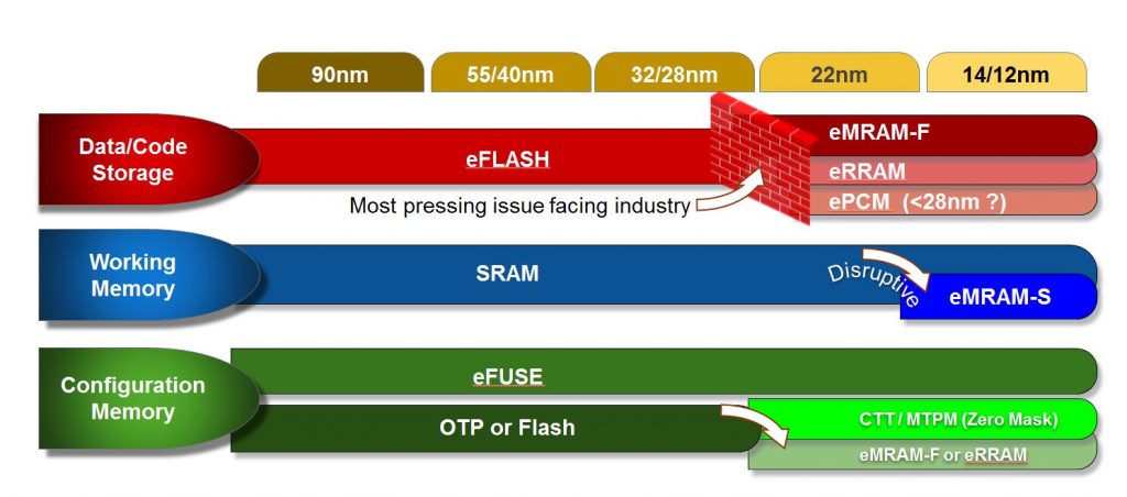
Right now, GlobalFoundries (and other contract makers of semiconductors) use eFlash (embedded flash) for chips that need relatively high-capacity onboard storage. This technology has numerous limitations, such as endurance and performance when manufactured using today's advanced logic technologies (i.e., sub-20nm nodes), which is something that is required of embedded memories. This is the main reason why GlobalFoundries and other chipmakers are looking at magneto resistive RAM (MRAM) to replace eFlash in future designs as it is considered the most durable non-volatile memory technology that exists today that can be made using contemporary logic fabrication processes.
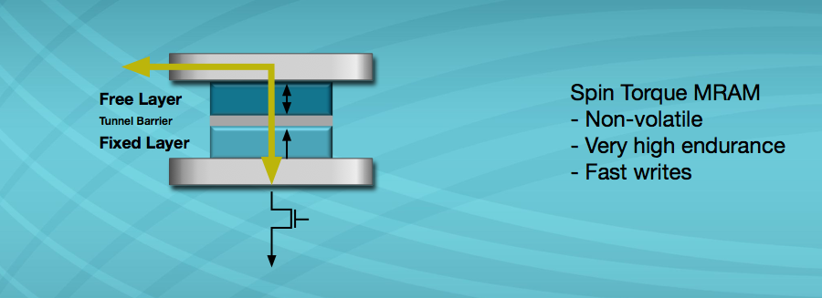
MRAM relies on reading the magnetic anisotropy (orientation) of two ferromagnetic films separated by a thin barrier, and thus does not require an erase cycle before writing data, which makes it substantially faster than eFlash. Furthermore, its writing process requires a considerably lower amount of energy. On the flip side, MRAM’s density is relatively low, its magnetic anisotropy decreases at high temperatures and performing write operations at low temperatures requires high currents (and if anisotropy is increased in general, it will require high currents even at not-so-low temperatures), which makes it a no-option for numerous applications, but which is still very promising for the majority of use cases that do not involve low temperatures.
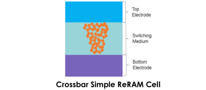
This brings researchers to ReRAM, which relies on changing the resistance across a dielectric material (from ‘0’ to ‘1’ or otherwise) by electrical current. The technology also doesn't require an erase cycle, promises very high endurance, and — assuming that the right materials are used — can work at a wide range of temperatures. Meanwhile, alloys used for ReRAM should be very stable in general in a bid to survive millions of switches and retain data, even when memory cells are produced using 'thin' moden fabrication processes (e.g., GF's 12LP or 12FDX). Finding the right substances for ReRAM will be the main topic of NTU’s research, whereas GlobalFoundries will have to find a cost-efficient way to produce the new type of memory at its facilities if the research is successful.
For years to come, GlobalFoundries (and its rivals) will use MRAM for a wide variety of applications as the technology is mature enough, fast enough, and durable enough. The company’s eMRAM implementation ‘integrates well’ with both FinFET and FD-SOI process technologies (although FinFET implementation is not yet ready), the company says, so expect it to be used widely. According to the foundry, it has multiple 22FDX eMRAM tape outs planned for 2019 and 2020.
GlobalFoundries is not standing still and is evaluating several eNVM technologies for its roadmap beyond 2020, including ReRAM. The company does not expect the research to come to fruition before 2021, but it certainly hopes that ReRAM will become another useful embedded memory technology.
It is noteworthy that companies like Western Digital are working on ReRAM-based storage class memory (SCM) to compete against Intel’s 3D XPoint and other SCM technologies. SCM-class ReRAM will have its differences when compared to embedded ReRAM that GlobalFoundries is particularly interested in, which once again shows that the technology could be applied very widely.
Related Reading:
- Microsemi Licenses Crossbar ReRAM Non-Volatile Memory
- Western Digital to Use 3D ReRAM as Storage Class Memory for Special-Purpose SSDs
- Phison’s Next-Gen eSSD Controllers to Support Everspin’s STT-MRAM Caching
- Sage Microelectronics To Introduce Enterprise SSD Controller Supporting STT-MRAM
- Everspin Begins Production of 1Gb STT-MRAM
- Samsung Ships First Commercial Embedded MRAM (eMRAM) Product
Sources: GlobalFoundries, Crossbar, Everspin, ChannelNewsAsia


6 Comments
View All Comments
name99 - Monday, October 28, 2019 - link
"its magnetic anisotropy decreases at low temperatures"Uh, the decrease is at high temperatures. It's very hard to imagine any sort of physics that reduces anisotropy (and similar non-heterogeneity) as temperatures get LOWER.
name99 - Monday, October 28, 2019 - link
But apart from that technical correction, I appreciate AnandTech keeping us all up to date with the (oh so slow, but happening) transition to newer memory types.rahvin - Monday, October 28, 2019 - link
These technologies are a major shift. You don't do those overnight, NAND took multiple years (close to a decade) to go from the lab to the foundry and it used the same silicon process tech that's used for everything else. You take something like the MRAM talked about above and now you are doping materials like ferrous layers into the process that have never been used with silicon microprocessor fabrication.Any major shift like this always results in something falling out of the attempts to mass produce it that complicates the production. All the new memory tech that's been proposed use processes or materials that aren't in use today, so the unknown is always can they be mass produced at reasonable costs. It takes a lot of time to figure things like that out, particularly where you are adding in methods or materials that have never been used in these industries before.
But when they do figure it out and demonstrate it's financially possible at industrial scale watch out, it'll probably take off like a bullet.
Diogene7 - Monday, October 28, 2019 - link
One key enabler that pull-in the need is likely the standardisation by JEDEC of the NVDIMM-P standard (that may be completed in 2020 ?).Regarding the choice of Globalfoundries for ReRam, personally, I prefer Carbon Nanotubes RAM (NRAM) from Nantero, which from the claims done by Bill Gervasi, on paper, seems one of the best option (but without all the data, it is difficult to know if there aren’t some critical data omitted in a way that is msleading).
It takes approx ~1 year and half / 2 years between the completion of a new standard, and being to use to buy the 1st products that use a standard (ex: PCI-e 4 standardized in 2017, some products available in 2019).
Therefore, if the JEDEC NVDIMM-P standard is completed in 2020, we could hope to see in ~H2 2022 / 2023 begins to appear on the market, likely first in server for data centers (there is a big market for it, and DC are likely ready to pay a premium for it)
rahvin - Monday, October 28, 2019 - link
Like all the other 'possibles' the carbon nanotube might work great in a lab but it could fall on it's face when they try to mass produce it.As I mentioned, one of the reasons NAND took off was it's made using the same processes as everything else. ReRam IIRC uses mostly traditional fab processes with an additional doping layer. MRAM uses most of a traditional silicon process but tosses in ferrous materials and some additional steps that I don't think tools exist for. The Spin-Torque stuff takes it a layer further and brings in quantum layering processes. Carbon nanotubes typically involve a process of super heating acetylene gas to vapor deposit carbon tubes (huge safety issues for such a process at industrial scale).
Each step away from traditional silicon lithography significantly complicates the manufacturing. Some of these possibilities you are potentially looking at building an entire toolchain, in other words not just building the RAM but also needing to build all the tools to build the chips. And for something like carbon nanotubes you might need to even build the tools to build the tools that will build the chips. Each step further from existing process makes it that much harder to bring it to industrial production, and even to verify you can do it economically.
With a new memory using traditional silicon lithography you can go into an existing factory and test your process ideas like they are proposing with ReRam at GF. But you get into these more exotic RAM's and you need to build a factory to test if you can build the stuff economically.
Anyway, my point is what drives this isn't some future standard, it's whether they can build the stuff at scale at a profit and mostly if someone can get the funding to test whether industrial production is feasible. Get an exotic memory with new production tech and you might need to spend a billion dollars just to verify you can build it at industrial scale.
Diogene7 - Sunday, April 12, 2020 - link
I understand the reasoning, but I would tend to think that a technology has better chance to get into High Volume Manufacturing (HVM) if there is a standard around the technology, as it could enable a higher Total Adressable Market (TAM).The standard JEDEC NVDIMM-P standard will finally enable the use of many different kind of Non Volatile Memory (NVM) like MRAM, ReRAM, Carbon Nanotubes RAM (NRAM),... on the memory bus instead of only DDR4 or DDR5 RAM...
Therefore it will create a much bigger market opportunity for different kind of NVM addressing different system needs, and therefore create for manufacturers a more compelling financial reason to invest in the manufacturing of those NVM