Arm Unveils 2024 CPU Core Designs, Cortex X925, A725 and A520: Arm v9.2 Redefined For 3nm
by Gavin Bonshor on May 29, 2024 11:00 AM EST- Posted in
- CPUs
- Arm
- Smartphones
- Mobile
- SoCs
- Cortex
- 3nm
- Armv9.2
- Cortex-A520
- Cortex X925
- Cortex A725
Arm Cortex A520: Same 2023 Core Optimized For 3 nm
The Arm Cortex-A520 isn't architecturally different, nor has it been changed compared with last year's TCS2023 introduction. Instead, it has been optimized for the latest 3 nm process technology, enhancing its efficiency and performance. This core, part of the second-generation Armv9.2 architecture, delivers some additional compute power for everyday tasks in mobile and embedded devices while maintaining peak levels of energy efficiency and reducing power consumption expected from Arm's smallest core.
These architectural tweaks ensure that the Cortex-A520 can maximize the potential of the 3 nm process, achieving higher transistor density and better overall performance without any significant changes to its fundamental design.
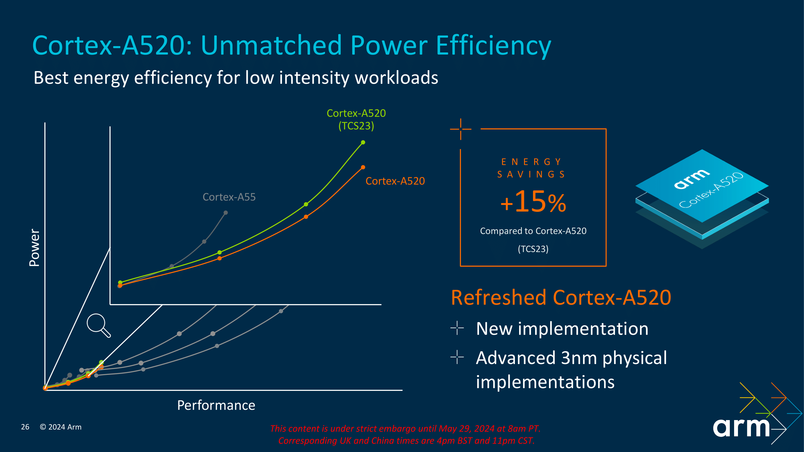
The Cortex-A520 showcases a significant 15% energy saving compared to the Cortex-A520 (TCS23). This improvement is critical for devices with prolonged battery life, such as smartphones and Internet of Things (IoT) devices. By optimizing power consumption, the Cortex-A520 ensures efficient performance without compromising energy usage.
The graph on the above slide clearly illustrates the relationship between power and performance for the Cortex-A520 compared to its predecessor, the Cortex-A55, and the previous Cortex-A520 (TCS23). The latest Cortex-A520 explicitly designed for the 3 nm notably improves power efficiency across various performance levels. This means that the Cortex-A520 consumes significantly less power for a given performance point, demonstrating Arm's commitment to providing performance gains across 2024's Core Cluster and focusing on refining things from a power standpoint to the smallest of the three Cortex cores.


55 Comments
View All Comments
SarahKerrigan - Wednesday, May 29, 2024 - link
"The core is built on Arm's latest 3 nm process technology, which enables it to achieve significant power savings compared to previous generations."ARM doesn't have lithography capabilities and this is a synthesizable core. This sentence doesn't mean anything.
meacupla - Wednesday, May 29, 2024 - link
AFAIK, the core design needs to be adapted to the smaller process node, and it's not as simple as shrinking an existing design.Ryan Smith - Wednesday, May 29, 2024 - link
Thanks. Reworded.dotjaz - Wednesday, May 29, 2024 - link
"ARM doesn't have lithography capabilities and this is a synthesizable core"And? Apple also doesn't have litho. You are telling me they can't implement anything with external foundries? Do you even know the basics of modern chip design? DTCO has been THE key to archieve better results for at least half a decade now.
Also this is clearly not just a synthesizable core. ARM explicitly announced this is avaiable as production ready cores, that means the implementations are tied to TSMC N3E and Samsung SF3 via DTCO, and this is the first time ARM has launched with ready for production hard core implementation.
You clearly didn't understand, and that's why it didn't mean anything TO YOU, and probably had to be dumbed down for you.
It actually makes perfect sense to me.
lmcd - Wednesday, May 29, 2024 - link
There was a turnaround time slide that didn't get Anandtech text to go with it that made this more clear, but a skim would miss it.zamroni - Monday, June 17, 2024 - link
it means the logic circuit is designed for 3nm's characteristics, e.g. signal latency, transistor density etc.older cortex designs can be manufactured using 3nm but it won't reach same performance as they were designed to cater higher signal latency of 4nm or older generations
Duncan Macdonald - Wednesday, May 29, 2024 - link
Lots of buzzwords but low on technical content. Much of this reads like a presentation designed to bamboozle senior management.Ryan Smith - Wednesday, May 29, 2024 - link
Similar sentiments were shared at the briefing.continuum - Thursday, May 30, 2024 - link
Whole tone of this article feels like it was written by an AI given how often (compared to what I'm used to in previous articles on this from Anandtech!) certain sentiments like "3nm process" and other buzzwords are used!name99 - Wednesday, May 29, 2024 - link
Not completely true...Interesting points (relative to Apple, I don't know enough about Nuvia internals to comment) include
- 4-wide load (vs Apple 3-wide load) is a nice tweak.
- 6-wide NEON is a big jump. Of course they have to scramble to cover that they STILL don't have SVE or SME; even so there is definitely some code that will like this, and the responses will be interesting. I can see a trajectory for how Apple improves SME and SSVE as a response, probably (we shall see...) also boosting NEON to 256b-SVE2. (But for this first round, still 4xNEON=2xSVE2)
Nuvia, less clear how they will counter.
Regardless I'm happy about both of these and requiring a response from Apple which, in turn, makes M a better chip for math/science/engineering (which is what I care about).
They're still relying on run-ahead for some fraction of their I-Prefetch. This SOUNDS good, but honestly, that's a superficial first response and you need to think deeper. Problem is that as far as prefetch goes, branches are of two forms – near branches (mostly if/else), which don't matter, a simple next line prefetcher covers them; and far branches (mostly call/return). You want to drive your prefetcher based on call/return patterns, not trying to run the if/else fetches enough cycles ahead of Decode. Apple gets this right with an I-prefetcher scheme that's based on call/return patterns (and has recently been boosted to use some TAGE-like ideas).
Ultimately it looks to me like they are boxed in by the fact that they need to look good on phones that are too cheap for a real NPU or a decent GPU. Which means they're blowing most of their extra budget on throughput functionality to handle CPU-based AI.
Probably not the optimal way to spend transistors as opposed to Apple or QC. BUT
with the great side-effect that it makes their core a lot nicer for STEM code! Maybe not what marketing wanted to push, but as I said, I'll take it as steering Apple and QC in the right direction.
I suspect this is part of why the announcement comes across as so light compared to the past few years – there simply isn't much new cool interesting stuff there, just a workmanlike (and probably appropriate) use of extra transistors to buy more throughput.