TSMC Tech Day 2020

One of the main drivers for the semiconductor industry is the growth in always-connected devices that require silicon inside, either for compute, communication, or control. The ‘Internet of Things’ era, depending on who you speak to, is set to scale to many billions of devices and subsequently many billions of dollars in opportunities. In order to drive this segment, semiconductor foundries have been developing cost-effective low power process node technologies for its customers to help drive a new level of power efficiency and low cost implementations. TSMC’s newest process targeting this market was announced at its 2020 Technology Symposium, and is to be called N12e. TSMC’s roadmap for its low powered platforms has centered around popular process node technologies optimized for low power and low...
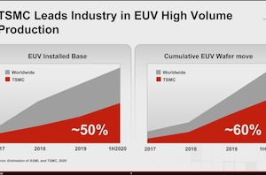
TSMC: We have 50% of All EUV Installations, 60% Wafer Capacity
One of the overriding central messages to TSMC’s Technology Symposium this week is that the company is a world leader in semiconductor manufacturing, especially at the leading edge process...
32 by Dr. Ian Cutress on 8/27/2020
TSMC and Graphcore Prepare for AI Acceleration on 3nm
One of the side announcements made during TSMC’s Technology Symposium was that it already has customers on hand with product development progressing for its future 3nm process node technology...
2 by Dr. Ian Cutress on 8/27/2020
Where are my GAA-FETs? TSMC to Stay with FinFET for 3nm
As we passed that 22nm to 16nm barrier, almost all the major semiconductor fabrication companies on the leading edge transitioned from planar transistors to FinFET transistors. The benefits of...
37 by Dr. Ian Cutress on 8/26/2020
2023 Interposers: TSMC Hints at 3400mm2 + 12x HBM in one Package
High-performance computing chip designs have been pushing the ultra-high-end packaging technologies to their limits in the recent years. A solution to the need for extreme bandwidth requirements in the...
35 by Andrei Frumusanu on 8/25/2020
TSMC Expects 5nm to be 11% of 2020 Wafer Production (sub 16nm)
One of the measures of how quickly a new process node gains traction is by comparing how many wafers are in production, especially as that new process node goes...
13 by Dr. Ian Cutress on 8/25/2020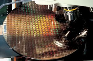
TSMC’s Version of EMIB is ‘LSI’: Currently in Pre-Qualification
Whilst process node technologies and Moore’s Law are slowing down, manufacturers and chip designers are looking to new creative solutions to further enable device and performance scaling. Advanced packaging...
19 by Andrei Frumusanu on 8/25/2020
TSMC Teases 12-High 3D Stacked Silicon: SoIC Goes Extreme
I’ve maintained for a couple of years now that the future battleground when it comes to next-generation silicon is going to be in the interconnect – implicitly this relies...
15 by Dr. Ian Cutress on 8/25/2020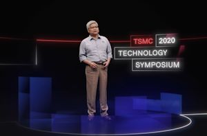
TSMC Updates on Node Availability Beyond Logic: Analog, HV, Sensors, RF
Most of the time when we speak about semiconductor processes, we are focused on the leading edge of what is possible. Almost exclusively that leading edge is designed for...
3 by Dr. Ian Cutress on 8/25/2020
‘Better Yield on 5nm than 7nm’: TSMC Update on Defect Rates for N5
One of the key metrics on how well a semiconductor process is developing is looking at its quantitative chip yield – or rather, its defect density. A manufacturing process...
107 by Dr. Ian Cutress on 8/25/2020


