Micron 3D NAND Status Update
by Billy Tallis on February 12, 2016 10:00 AM EST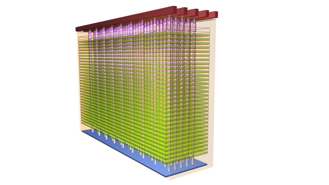
Update: We've got some more information and diagrams from Micron's Winter Analyst Conference earlier today.
After samples of their upcoming 3D NAND were sighted in the wild at CES, Micron has taken the time to provide some details about the flash memory and their plans for it. A lot of this is a recap of information we've previously covered, but we've got some new details and a better idea of the roadmap for the future.
The entire flash memory industry has shifted focus to the devlopment of 3D NAND flash memory as the replacement for planar NAND flash memory. Samsung took an aggressive approach and has enjoyed some great success with their V-NAND branded 3D NAND, but it hasn't been an entirely trouble-free transition. Micron has been more conservative both in technology and timing, but they plan on having a strong competitor on the market later this year.
Micron's first generation 3D NAND takes the form of a 256Gb MLC die and a 384Gb TLC die (compare with their 128Gb 16nm MLC and TLC). At a high level, the die will be partitioned into four separate planes, compared to two planes for most competing NAND. A 480GB drive using the four-plane 256Gb dies will have access to approximately the same amount of parallelism as a 480GB drive using two-plane 128Gb dies, so this capacity jump won't bring the performance drops that have tarnished some NAND process shrinks.
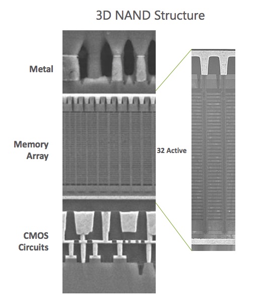
The key development that allows Micron to produce a four-plane die without inflating die size and cost relative to the two-plane competition is that they've layered much of the required additional circuitry under the 3D flash array, instead of sitting alongside. Micron says that their "CMOS Under the Array" design puts more than 75% of the logic (things like address decoding and page buffers) under the flash memory. It doesn't make the additional segmentation of the four-plane design entirely free, but it allows it to be a very cost effective performance optimization. This is still planar CMOS logic, not any kind of 3D or stacked logic; it's just got some metal interconnect layers and the flash array piled on top.
On a smaller scale, the 3D NAND will have a page size of 16kB and erase block sizes of 16MB for the MLC and 24MB for the TLC. Because CPUs and filesystems are still mostly dealing with 4kB chunks, Micron has included a partial page read capability that allows for a 4kB read to be done a bit faster and with about half the power of a full 16kB page read. This helps offset some of the penalty the larger page size can have on random 4kB read performance. The large erase block sizes won't have much of a direct impact on performance and are a necessary efficiency measure: erasing requires charge pumps to produce higher voltages than reads or writes use, and it's a slower and more power-hungry operation. If you're going to fire up that extra circuitry and block access to the entire plane for 1ms or more, you might as well erase a usefully large amount of flash.
For the architecture of the individual memory cells, we have nothing new to report. Intel and Micron are alone in their decision to stick with floating-gate flash technology instead of transitioning to charge-trap flash. We've previously explained how the technologies differ and what kinds of advantages the manufacturers want to reap from the change. The cost is that the design process involves different tradeoffs that are not as thoroughly explored and understood as the dynamics of floating-gate flash, and for now Micron is sticking with what they know. Micron's 3D NAND might not have the best write endurance, but they're expecting to have an advantage in data retention time for healthy flash. They aren't providing exact numbers, but they're estimating that drives relying on simpler BCH ECC can get effective program-erase cycle lifetimes in the thousands and drives with LDPC will have effective cycle counts of tens of thousands. Once the process has matured it should exceed their 20nm planar NAND's write endurance.
The first 3D NAND Micron has ready for the market will produced to the endurance standards for client drives, with enterprise-grade 3D NAND following later. The MLC is currently a few weeks ahead of the TLC in the qualification process, but given the state of the client SSD market the TLC will be the more popular product and will overtake the MLC in volume produced within a few months of 3D NAND drives hitting the market. Overall their 3D NAND will comprise a majority of their flash output on a per-GB basis by the second half of 2016. Micron is sampling drives with 3D NAND to partners this month and is planning for general availability in June. Other drive vendors using Micron's NAND will be on similar release schedules.
Micron hasn't announced any specific drive models, but they've given a general roadmap that is unsurprising. Consumer and client products will come during the middle of the year, with the capacity and cost improvements allowing for things like 2TB 2.5" drives and 1TB single-sided M.2 drives. Toward the end of 2016 and into 2017 we'll see enterprise products such as very high capacity (8TB+) drives and updates in the existing product segments for SAS and PCIe drives.
Looking further to the future, Micron gave a presentation last week at the IEEE International Solid-State Circuits Conference entitled "A 768Gb 3b/cell 3D-Floating-Gate NAND Flash Memory". This was more about bragging about their R&D in an academic context than announcing any concrete future product plans, but it does represent the most likely successor to their first-generation 3D NAND. The chip in question provides a whopping 768Gb (96GB) capacity when operated as TLC, and 512Gb (64GB) as MLC. The die size is about the same as their 32-layer 384Gb TLC, the areal bit density is almost doubled, and most of the other details are the same—implying that the layer count has probably increased, though Micron isn't saying how many layers it uses. If Micron has plans to switch to charge-trap flash they're keeping it under wraps for now, and any such transition isn't imminent. The second-generation 3D NAND will start production in their Singapore fab this summer, and volume will be ramping up around the end of 2016 (during the second quarter of their fiscal year 2017). Micron predicts their second-generation 3D NAND will be at least 30% cheaper per Gb than the first generation, which they report to be at least 25% cheaper than their 16nm planar NAND.
Source: Micron


19 Comments
View All Comments
jjj - Friday, February 12, 2016 - link
Nice that it has 4 planes, with 48GB TLC dies i was wondering about perf per SSD capacity.The 768Gb , capacity wise, seems in line with what others will have. Do wonder if we see any 4 bit per cell in 2017 or that's too soon. 16GB xpoint + 64GB 4 bit NAND with just 2 dies would be fun in a phone.
extide - Friday, February 12, 2016 - link
How does 768Gb, capacity wise, seem in like with what others will have? I don't think anyone has announced anything bigger than 256Gb ? Maybe I missed something? That seems like a WAY bigger die than pretty much anyone else has said anything about.jjj - Friday, February 12, 2016 - link
Others do have 768Gb on their roadmaps in 2017 so even if this will be gen 2 for Micron (it's not clear yet that it is), it is in line with (some) others., capacity wise. The precise timing fort each remains to be seen.And don't forget that die size is a factor too. Micron has a big die, Sandisk/Toshiba for example have smaller capacity now but in a smaller die that can fit in a microSD.
willis936 - Friday, February 12, 2016 - link
I can't imagine xpoint controller's being power efficient enough to have a noticeable increase in performance over nvme/half amplitude pcie (as is done in the 6s). I'd say that second die would be put to better use doubling storage :Djjj - Friday, February 12, 2016 - link
Can't say i have a clue about the xpoint controller and what perf and power it can get.In phones one of the main goals would be to get rid of some or all RAM for a big gain in battery life- no idea how they plan to implement it and before we have more details it is futile to speculate.
As for 16GB, xpoint gen 1 die is 16GB so the option of using less is not there.
name99 - Friday, February 12, 2016 - link
XPoint replacing RAM (as opposed to replacing flash) requires- appropriate ordering instructions in the instruction set (ARM or x86)
- OS modifications to use these instructions
ARMv8.2A includes the appropriate instructions, but there are no implementations yet, and it seems unlikely that these will arrive before at earliest H2 2017. (A72 isn't yet out there, and as far as I know Kyro is ARMv8.0A. Apple MAY ship the A11 as 8.2A, but for various reasons I think the A10 is just a slightly faster, slightly improved A9 --- like the A7 to A8 transition.)
Intel seems unlikely to get those instructions into Atoms or even mobile before they get them into Xeon, and likewise to do their usual clusterfsck of supporting them so randomly across processors that it will be ten years before anyone can rely on them.
So no CPUs in the near future, which means that even if Android ARE working on this support in the OS, they can't push it out (or even test it) for a while --- and when it comes to storage you want to test a LOT on REAL hardware before you ship it into the field.
So it's certainly coming, but I'd be amazed if I saw it in Android before 2019 or so. Apple COULD have it as early as 2017 because their tight integration means they could even have test silicon in house right now. It would be worth looking at the storage talks at WWDC this year and next year to see if they provide any hint as to ways of doing things that most make sense on an NVM design.
[It's also possible, and even makes a kind of grand sense, that it's at the transition to an NVM design --- NVM hardware, NVM OS, NVM APIs --- that it makes the most sense to perform the Mac switch to ARM. If this gives Macs a substantial boost in "user-level" performance, even if CPU performance temporarily goes backwards a little, the transitions would be a little smoother; and it's the sort of thing that would be vastly easier to do with an Apple-designed CPU that while waiting on Intel's timetable.]
jjj - Saturday, February 13, 2016 - link
When i mentioned xpoint it was a 2017 matter, and that at best.Anyway, xpoint in anything is a 2017 matter , it won't ship much , if any this year. In phones it is expected that it will take a bit longer than in server and PC SSD, because of the extra complications. It might even be unlikely for gen 1 to get in phones because of the price. They might actually be aiming for SoCs built to work with it, maybe advanced packaging but i would rather not speculate on this before we have proper specs. Oh, and i did say some or all RAM. Some phones this year will have 6GB of RAM, one option would be to cut just some of that and add xpoint and maybe hide it from the OS - kinda like Marvell's FLC i guess, except they do it on NAND.
phoenix_rizzen - Monday, February 15, 2016 - link
There's a couple of phones out already (or have been reviewed with shipments coming very soon) with Cortex-A72 cores inside. Mostly MediaTek SoCs, I believe.fishjunk - Friday, February 12, 2016 - link
What does this mean for the future price/capacity of SSDs?hojnikb - Friday, February 12, 2016 - link
this means cheaper and more durable ssds