AMD Unveils GPU Architecture Roadmap: After Polaris Comes Vega
by Ryan Smith on March 15, 2016 3:30 AM ESTAlthough AMD’s GDC 2016 “Capsaicin” event was primarily focused on game development – it is the Game Developers Conference, after all – AMD did spend a brief moment discussing their future GPU plans. For the first time in many years, AMD has published a GPU architecture roadmap.
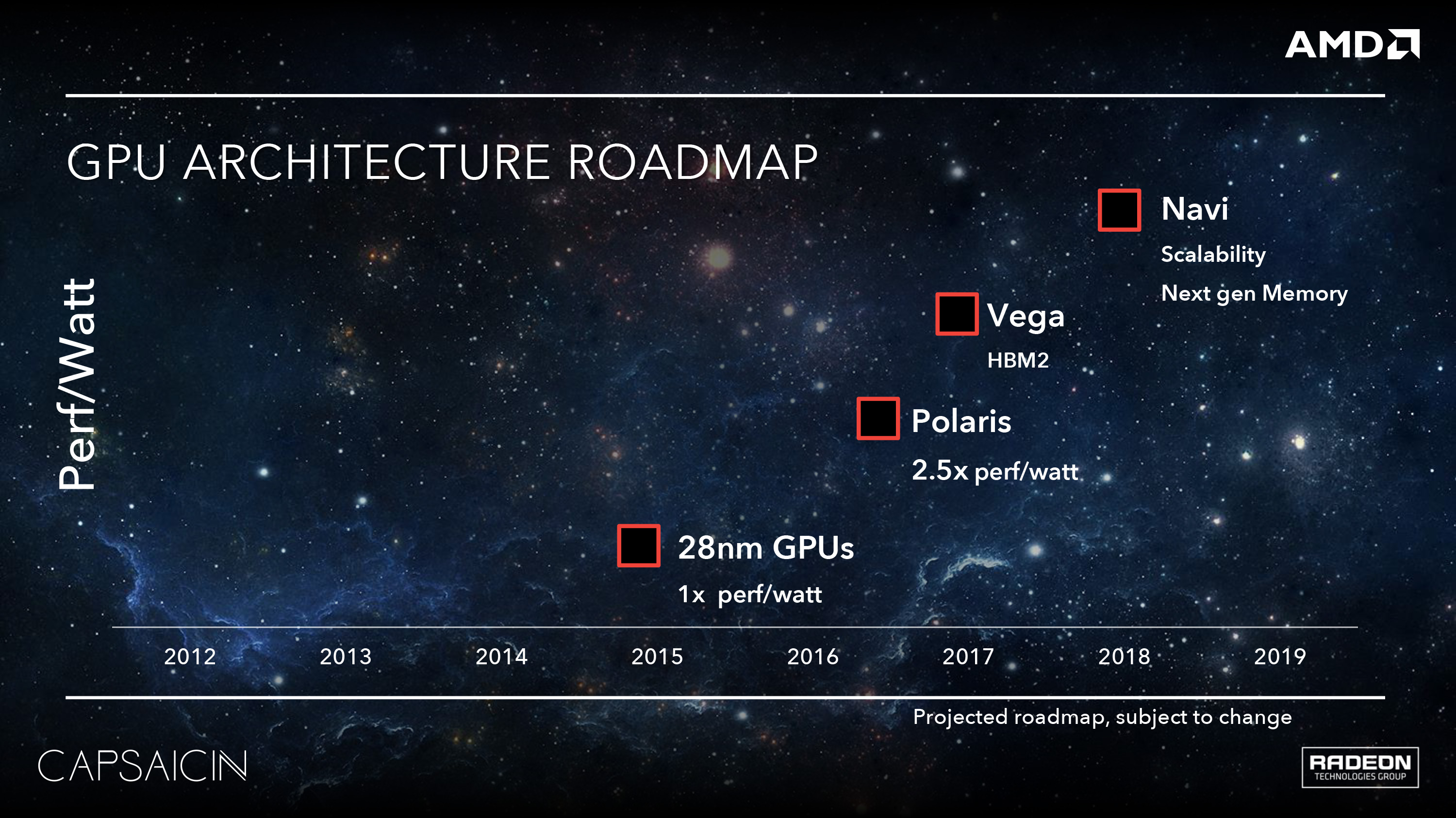
Plotting perf/watt against the years, AMD’s roadmap unveils two new architectures: Vega, and Navi. Essentially everything there is to know about these architectures is in this slide – AMD is being tight-lipped regarding further details – but this map gives us some tantalizing new information to work with.
Vega is currently scheduled to come relatively quickly after Polaris. Depending on how literal you interpret this chart, the far left edge of the Vega box does fall into 2016, though obviously AMD intends to leave themselves some wiggle room here and not tie themselves down to specific dates. The fact that Vega comes this soon after Polaris is interesting; it seems hard to believe that it’s a direct successor to Polaris – I can’t see AMD replacing Polaris parts in less than a year – so this points to Vega being more of a cousin, and is where AMD’s naming system isn’t especially helpful in deciphering anything further.
With Polaris confirmed to use GDDR5, Vega is notable for being the first AMD architecture to use HBM2, and the first parts in general to use HBM tech since Fiji. I’m presuming these are higher-end GPUs to complement the Polaris GPUs (the smaller of which we know to be a low-power laptop design), which is where HBM would be more cost-effective, at least at current prices.
Meanwhile AMD has also confirmed the number of GPUs in the Vega stack and their names. We’ll be seeing a Vega 10 and a Vega 11. This follows Polaris GPU naming – which has finally been confirmed – with Polaris 10 and Polaris 11. I have also been told that Polaris 11 is the smaller of the Polaris GPUs, so at this point it’s reasonable to assume the same for Vega.
Finally, farther out towards 2018 is an architecture AMD is calling Navi. This one I suspect will attract the most attention (even if it’s the farthest out) due to the ambiguity of its features: “scalability” and “next gen memory”. Similar to how it’s hard to see Vega directly replacing Polaris, it’s hard to see Navi directly replacing Vega after only a year. This leaves Navi rife for speculation; I could very well see it being a Polaris replacement since we’ll be nearly 2 years past Polaris, or perhaps something to do with AMD’s APU plans. Either way I don’t expect that this will be the last time AMD teases it before finally launching it.


54 Comments
View All Comments
jjj - Tuesday, March 15, 2016 - link
Not that it would be in any way unexpected but that roadmap seems to indicate that they'll skip 10nm.They can offer enough perf per $ gains on 14/16nm with Vega due to lower costs and HBM2, instead of going 10nm very early.
By mid 2018, 7nm should be available so hard to imagine Navi would go 10nm.
emn13 - Tuesday, March 15, 2016 - link
So you're betting 7nm will be ready for mass-release in mid 2018? That sounds optimistic to me...jjj - Tuesday, March 15, 2016 - link
I am not betting, i am concluding. As for 7nm, it could be ready well before that, mid 2018 wouldn't be that early.From your tone I do understand that you are a TSMC hater (apparently those exist for some reason ) but the way TSMC does it, the 7nm transition could be quick.TSMC is pairing processes and reusing the vast majority of tools. 20 with 16 and 10 with 7nm.
Additionally , 10nm brings only 15% speed gains over 16 and that's not worth it in GPU when you can just go wider.
So yeah, i am concluding that they will skip 10nm and Navi will be on 7nm,whenever it arrives.
SaberKOG91 - Tuesday, March 15, 2016 - link
I doubt they are a "TSMC Hater", it is simply that process transitions have been steadily slowing down, year by year. Whether you realize it or not, 5nm is the lower limit of electron-tunneling based designs. At that point, it is not possible to prevent an electron from existing on both sides of the channel, purely based on its size.saratoga4 - Tuesday, March 15, 2016 - link
I don't think whatever TSMC brands as "7 nm" is going to have anything to do with the 5x10^-9 meter limit you're referring to. Probably they will take whatever is ready to go in that time frame and then push it out. Fabs are business, they need a regular product refresh, and they'll likely have one.SaberKOG91 - Tuesday, March 15, 2016 - link
Below the 7nm channel width (around 5nm) it becomes impossible to ignore the effects of quantum tunneling effects. We will either need a radical new transistor design, or a bunch of quantum physicists designing our standard cell libraries.Either way, process scaling is slowing down, and there is no way that any process from TSMC (or any other fab) will make it to high enough yields to be useful by the end of 2018 for Navi.
ImSpartacus - Tuesday, March 15, 2016 - link
It sounds like 10nm would be another 20nm mess. Where are you finding this info?Shadow7037932 - Tuesday, March 15, 2016 - link
I seriously doubt we would have mass production at 7nm by 2018. We've only got 14nm for mainstream mass production recently.Kvaern2 - Tuesday, March 15, 2016 - link
When was the last time TSMC delivered a process on schedule?Michael Bay - Tuesday, March 15, 2016 - link
In 90s!jjj is insane anyway.