MediaTek Announces New Premium Helio P60 SoC
by Andrei Frumusanu on March 1, 2018 9:30 AM EST- Posted in
- Smartphones
- Arm
- Mobile
- Trade Shows
- MediaTek
- Mali
- Helio
- MWC 2018
- P60
- A73
- A53
- ARM Cortex
BARCELONA, ESP – Earlier this week MediaTek announced a new entry in the Helio SoC line-up, the Helio P60. The P60 comes with a strategy change for MediaTek as the company is doubling down on the super-midrange “premium” category and expanding that range into multiple sub-tiers.
The strategy change comes from market and lack of success in the high-end Helio X series. Last year’s Helio X30 had only a few design wins and was relatively late to market. MediaTek seems to have had a string of bad luck with the X20 and X30 as both came on either problematic or very delayed manufacturing process nodes which lost them important design wins. As more vendors switch over to custom designs in the high-end and Qualcomm puts more pressure with competitive designs, MediaTek decided to put a hold on the X series for now and concentrate in the range where it is very successful, the P series.
The this new segmentation means that the P60 doesn’t position itself as direct successor to late last year’s P23 and P30 but rather as a tier above them, hence the naming scheme.
| MediaTek Current P-Series | |||
| SoC | Helio P23 | Helio P30 | Helio P60 |
| CPU | 4x Cortex A53 @ 2.3GHz 4x Cortex A53 @ 1.65GHz |
4x Cortex A53 @ 2.3GHz 4x Cortex A53 @ 1.65GHz |
4x Cortex A73 @ 2.0GHz 4x Cortex A53 @ 2.0GHz |
| GPU | Mali G71MP2 @ 770MHz | Mali G71MP2 @ 900MHz | Mali G72MP3 @ 800MHz |
| APU / NPU / AI Proc. / Neural IP | - | 2x 140GMACs | |
| Memory | 1x 32bit LPDDR3 @ 933MHz 2x 16bit LPDDR4X @1500MHz |
2x 16bit LPDDR4X @ 1600MHz | 1x 32bit LPDDR3 @ 933MHz 2x 16bit LPDDR4X @ 1800MHz |
| ISP/Camera | 1x 24MP or 2x 13MP | 1x 25 MP or 2x 16MP | 1x 32MP or 2x 20+16MP |
| Encode/ Decode |
2160p30 H.264 | 2160p30 H.264 & HEVC | 2160p30 H.264 & HEVC |
| Integrated Modem | Category 6 DL = 300Mbps 3x20MHz CA, 64-QAM UL = 50Mbps 64-QAM |
Category 7/13 DL = 300Mbps 3x20MHz CA, 64-QAM UL = 150Mbps 2x20MHz CA,64-QAM |
Category 7/13 DL = 300Mbps 3x20MHz CA, 64-QAM UL = 150Mbps 2x20MHz CA,64-QAM |
| Mfc. Process | 16FFC | 16FFC | 12FFC |
The P60 is the first SoC in the P-lineup to employ “big” microarchitecture cores as it uses 4x Cortex A73 cores at up to 2.0GHz – a significant performance boost in performance over the P23 and P30’s A53 cores. The efficiency cores are naturally still Cortex A53’s and they run at the same 2.0GHz frequency as the performance cluster.
On the GPU side we see an update in the IP as MediaTek in turn transitions from G71 to G72. The P60 uses a G72MP3 running at up to 800MHz and promises a 25% gaming efficiency boost (at up to 70% higher GPU performance).
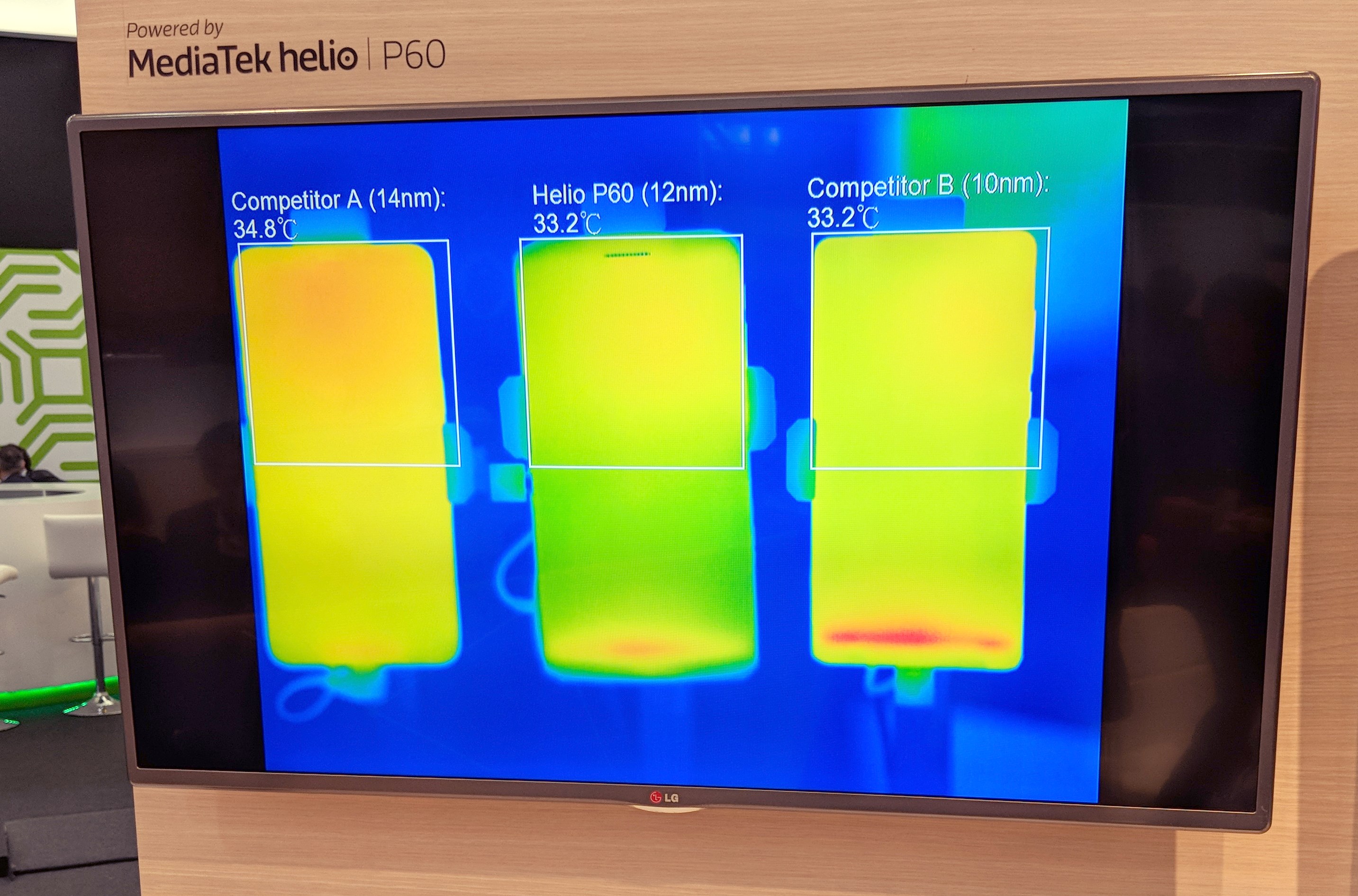
Snapdragon 660 vs Helio P60 vs Snapdragon 835 Thermal Comparison @ MWC2018
The P60 is the first mobile SoC to come manufactured on TSMC’s new 12nm 12FFC process node. 12FFC is a shrink of 16FFC and uses the same tools – it’s a cost effective alternative to the more expensive 10FF process which requires quad-patterning. While 12FFC does not quite achieve the die size reduction that 10FF would, it’s extremely competitive in terms of power characteristics and reaches near the same efficiency. I asked MediaTek about the company process roadmap plan and they will focus exclusively on 12FFC for 2018 and have no plans for further 10nm silicon. The next generation will jump directly to 7nm in mid 2019 (after other vendors) when mass production will have reached mature and cost-effective levels.
The P60 is the first SoC to bring dedicated neural network accelerators into the mid-range. MediaTek’s denomination for such IP is APU (AI Processing Unit) so that’s yet another term added to the varied basket of abbreviations from different companies. MediaTek wouldn’t disclose the IP provider but say’s it’s a dual-core implementation offering 2x140GMACs. MediaTek will offer a custom software stack called NeuroPilot which will be compatible with Google’s NN API and frameworks such as TensorFlow, TF Lite, Caffe and Caffe2.
The modem subsystem remains the same as on the Helio P30 – it supports LTE up to Category 7 with 3x20MHz CA and 300Mbps download speeds and Category 13 with 2x20MHz CA for up to 150Mbps upload speeds.
The Helio P60 is in production now and we should see consumer smartphones with the chipset available starting early Q2 2018.


74 Comments
View All Comments
ET - Thursday, March 1, 2018 - link
Can we call the AI Processing Unit and AIPU? Would be clearer.Mumrik - Thursday, March 1, 2018 - link
Is it me or does "Competitor B (SD835) look hotter in every area of the phone, yet have the same temperature? What are they getting at, or is that slide just bullshit?Colin1497 - Thursday, March 1, 2018 - link
The die is maintaining the same temperature doesn't mean that the surface of the phone is maintaining the same temperature. Better heat transfer can transfer more power out of the die and maintain the same temperature.Santoval - Friday, March 2, 2018 - link
You should take that thermal comparison "test" with a very large grain of salt. The bottom heat patch of the Competitor B phone is obviously due to it charging at the time, but it is unknown if the other two phones also draw power at the same time. Competitor A does not appear to be charging (its bottom is barely orange at all), while the Helio P60 phone also does not draw any power.I don't think the optical image of the three directly corresponds to their thermal image - I have no idea what these weird adaptors(?) are supposed to be. In any case, this "test" is not a thermal test at all, since for it to have any merit the three phones would need to be at the exact same state running the exact same thing. A mere thermal photo with zero other data is not a thermal test comparison.
BigDragon - Thursday, March 1, 2018 - link
Looks promising. I just need a list of phones that will contain these new processors. After the Snapdragon 808 and 810 debacle, I'd like to avoid Qualcomm.Dr. Swag - Saturday, March 3, 2018 - link
Because it's their fault that 20nm had really bad leakage...The 835 is perfectly fine. Pretty good power consumption too.
Plumplum - Saturday, March 10, 2018 - link
20nm fault?Helio X20 is able to run 10 cores nearly at full speed with 20nm process during 10minutes! Only loosing 6% performances...rumors are false on cpu, gpu lost about 30% (Many others lost 50% on the same test but nobody noticed!)
It's both cortex A57 and 20nm that doesn't work.
Both Huawei and mediatek refuse to release A57 (X10, kirin 930).
Qualcomm use it for scoring in benchmarks and release crappy soc.
All their first generation or 64bits was crap, 410, 615, 808, 810! But they managed to sell it (patents abuse?)
Then they use these problems to make people think their custom cores are better. They aren't (on both krait and kryo on 820).
New kryo are nearly the same as cortex A73/A53 on 660 (and probably A75/A55 on 845)
It's obvious that kryo on 660 or 835 is nearly nothing more than a Cortex A73, compare detailed score :
https://browser.geekbench.com/v4/cpu/7397584
https://browser.geekbench.com/v4/cpu/7397478
https://browser.geekbench.com/v4/cpu/7165483
Note : 835, kryo 280, 2.45ghz - 660, kryo 260, 2.2ghz - P60, cortex A73, 2.0ghz
ZolaIII - Thursday, March 1, 2018 - link
Meh still an entry lv GPU which will reach only 75% performance of A508~A509 and still use much more power. As usual QC counterpart (S635) will be much better in every day use & for light gaming not to mention long term support from CAF and availability of the kernel source. Still it may not be all grim for MTK we will see how will their Project Treble work for them as now they can skip most part the OEM's but I don't have high hopes. On the other hand it will have one advantage & that is pricing thanks to MTK recorded on doing so but more importantly because TSMC so called 12nm FinFET process is actually 15~20% cheaper (thanks to less employed layer masks) than TSMC 14 nm or Samsung 16nm one. Still I am eager to see products on GF 22nm FD-SOI that pushes that cost limit future 5~10% down (compared to 12nm FinFET), can push the power consumption even more down (back biosing) and most importantly it will put RF components power consumption down a lot (50~75% compared to today).serendip - Thursday, March 1, 2018 - link
Process node comparisons are almost meaningless now because each foundry has different ways of calculating feature size. Mediatek have been relegated to the bargain basement end of the market, their chips are dirt cheap but support is woefully lacking. They also haven't learned anything about GPL licensing and code release requirements either.How is it that other SoC vendors can integrate Mali GPUs with decent power profiles but Mediatek can't? They're way behind compared to Qualcomm's Adreno GPUs that perform better and use less power.
Retycint - Friday, March 2, 2018 - link
The weak GPU bit is only true for the X series though. Sure the mali is not as efficient as the adreno but the mali-t880mp2 in the helio P20 actually performs identically to the Adreno 506 in the SD625Source: https://www.gsmarena.com/sony_xperia_xa1_plus-revi...