Micron’s DRAM Update: More Capacity, Four More 10nm-Class Nodes, EUV, 64 GB DIMMs
by Anton Shilov on June 28, 2019 10:00 AM EST
During its earnings conference call with investors and financial analysts earlier this week, Micron expressed confidence in its long-term future and strong demand for its products as new applications emerge in various fields in the coming years. The company also outlined its plans to expand capacities and rapidly shift to more advanced process technologies.
“We are confident that the long-term demand outlook for memory and storage is compelling, driven by broad secular trends such as AI, autonomous vehicles, 5G, and IoT,” said Sanjay Mehrotra, CEO of Micron. “The new Micron is well positioned to take advantage of these trends, with innovative products, a responsive supply chain, and well-established relationships with customers worldwide.”
Prices of DRAM have declined rather dramatically in the recent quarters as supply exceeds demand. To cut down on costs and to prepare for the emergence of new applications that will need memory, DRAM makers are aggressively transitioning to newer process technologies. Meanwhile, while admitting that they need to balance DRAMs supply and demand, they actually set up aggressive plans for expansion for their production capacities because they need more cleanroom space for upcoming manufacturing technologies.
Micron has an aggressive roadmap when it comes to fabrication proceses that includes four more 10 nm-class nodes (i.e., for a total of six 10 nm class technologies), and the company is researching an eventual transition to extreme ultraviolet lithography (EUVL). That being said, the company is also expanding its production capacities in a bid to produce next-gen memories for next-gen applications. The company is currently exploiting the fruits of its latest process technology by preparing 32 GB memory modules for client systems as well as 64 GB DIMMs for servers.
32 GB and 64 GB Memory Modules
Earlier this month we discussed Micron’s 16 Gb DDR4 memory chips which are produced using the company’s 2nd Gen 10 nm-class fabrication process (also known as 1Y nm). These DRAM devices are already found on prototypes of 32 GB DDR4 unbuffered DIMMs for client systems from ADATA and Crucial. The memory modules will be hitting the market in the near future, though there is no a specific launch date as of yet.
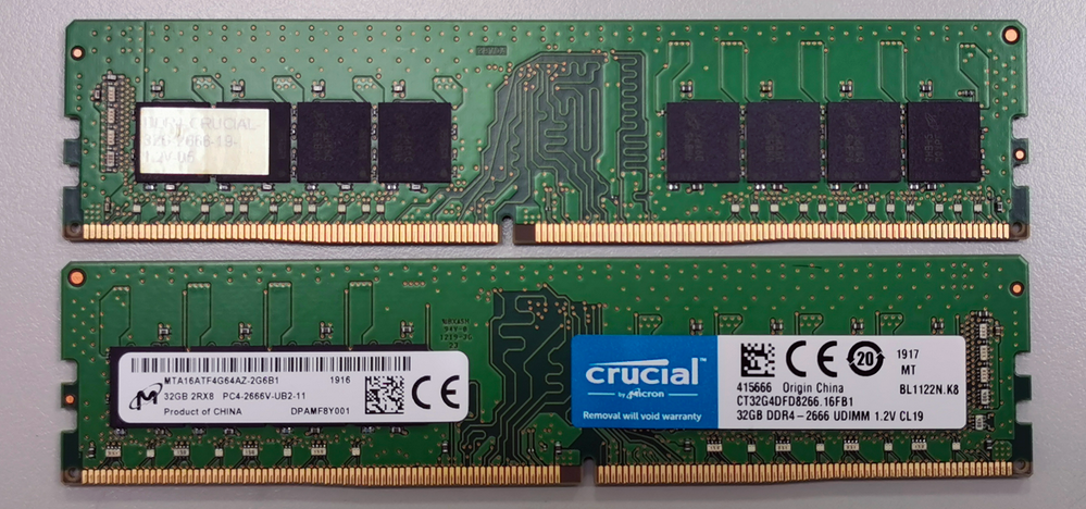
In addition to 32 GB UDIMMs for client systems, Micron is also preparing server-grade 64 GB registered DIMM based on the new 16 Gb chips. For servers, usage of 64 GB RDIMMs based on 16 Gb DRAM devices (produced using an advanced process technology) means a decrease in power consumption, which should be significant considering the fact that modern machines use massive amounts of memory. Samples of such modules are already available to customers for qualification, but it is not completely clear when they are set to ship.
Keeping in mind that 32 GB UDIMMs and 64 GB RDIMMs (based on 16 Gb DRAMs) are pretty rate, Micron’s Crucial will clearly be able to capitalize on semi-exclusive products.
New Capacities in Japan and Taiwan
Back in April, in a bid to prepare for increased demand for DRAM as well as new process technologies, Micron Memory Taiwan (former Rexchip Semiconductor) broke ground on its new cleanroom at its campus near Taichung, Taiwan.
Micron Memory Taiwan already makes 100% of its DRAM products using Micron’s 1st Gen 10 nm-class manufacturing technology (also known as 1X nm) and will move on straight to 3rd Gen 10 nm-class process (aka 1Z nm) in the near future. Meanwhile, last year Micron opened up a new testing and packaging facility near Taichung, creating one of the world’s only vertically integrated DRAM production facility.
In addition, Micron announced plans to spend $2 billion on a new cleanroom in its campus near Hiroshima, Japan. The new production capacity will reportedly be used to make DRAMs using Micron’s 13 nm process technology.
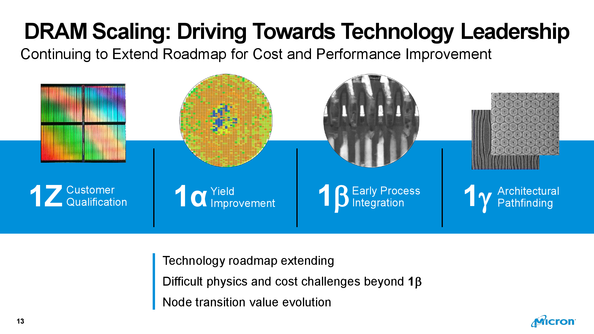
Aggressive Roadmap
As it gets increasingly harder to scale new manufacturing technologies (both in terms of engineering as well as financial challenges), Micron, like all DRAM manufacturers, is going to have multiple 10 nm-class nodes. In addition to 1st Gen and 2nd Gen 10 nm-class process technologies used today, Micron plans to introduce at least four more 10 nm-class fabrication processes: 1Z, 1α, 1β, and 1𝛾 (Greek gamma, not y), which are now in various stages of development.
Analysts from TechInsights say that Micron has quietly started to use a die shrink version of its 1X nm process technology known as 1Xs, which indicates that the total number of Micron’s 10 nm-class fabrication processes would be higher than six. Micron itself does not confirm this, but it says that it has R&D staff in all of its manufacturing facilities to ensure maximum yields (and other attributes), which could mean that there might be variations of the same node at different fabs.
At present, Micron is ramping up its 2nd Gen 10 nm-class fabrication process (aka 1Y nm) that is used to make a variety of products, including the company’s 12 Gb LPDDR4X as well as 16 Gb DDR4 memory devices.

The company’s next-generation 1Z nm is currently qualified by Micron’s customers (i.e., they are testing various chips produced using the process), it is expected to be announced in the near future and which is on track to ramp in Micron’s FY2020, which begins in September. This technology will be used to produce 16 Gb LPDDR4/LPDDR5 memory devices as well as DDR5 memory devices (according to TechInsights).
Following the 1Z nm node, Micron plans to start using its 1α nm manufacturing technology that is currently being tweaked for higher yields, meaning that it is in its later stages of development. After that comes Micron’s 1β nm fabrication process, which is in its early stages of development. In the meantime, the company’s engineers are in pathfinding mode for a viable architecture of its 1𝛾 nm technology.
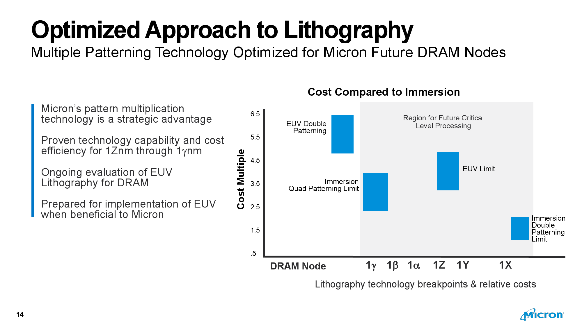
All of the firm’s 10 nm-class nodes announced so far rely on deep ultraviolet lithography (DUVL) with double, triple, or quadruple patterning. Micron is confident that all of the 10 nm-class processes currently in development — 1Z, 1α, 1β, and 1𝛾 nm — are cost efficient and technologically viable for years to come. Meanwhile, keep in mind that multi patterning requires more process steps, which makes production cycle longer and therefore more lithography tools and cleanroom space is needed to sustain existing output (i.e., wafer starts per month).
At the current pace of one new node per ~12 months, Micron’s multi patterning technology roadmap extends to at least 2023 (I am speculating here!) in terms of introduction of new nodes if all goes as planned. Keeping in mind that every new process technology is used for at least three to four years, it is safe to say that Micron plans to use multi patterning DUV technologies for many years to come.
Meanwhile, the company admits that there are tough physics and cost challenges beyond its 1β nm process as immersion lithography with quad-patterning faces its physical and economical limits at 1𝛾 nm process technology. That said, it remains to be seen what this node is set to bring to the market.
Micron and EUV
Micron does not say whether it will go straight to EUV after the 1𝛾 nm process. The company is evaluating capabilities of ASML’s Twinscan NXE step-and-scan as well as other equipment required for production using extreme ultraviolet lithography, and is assessing when these tools will be viable to make DRAM.

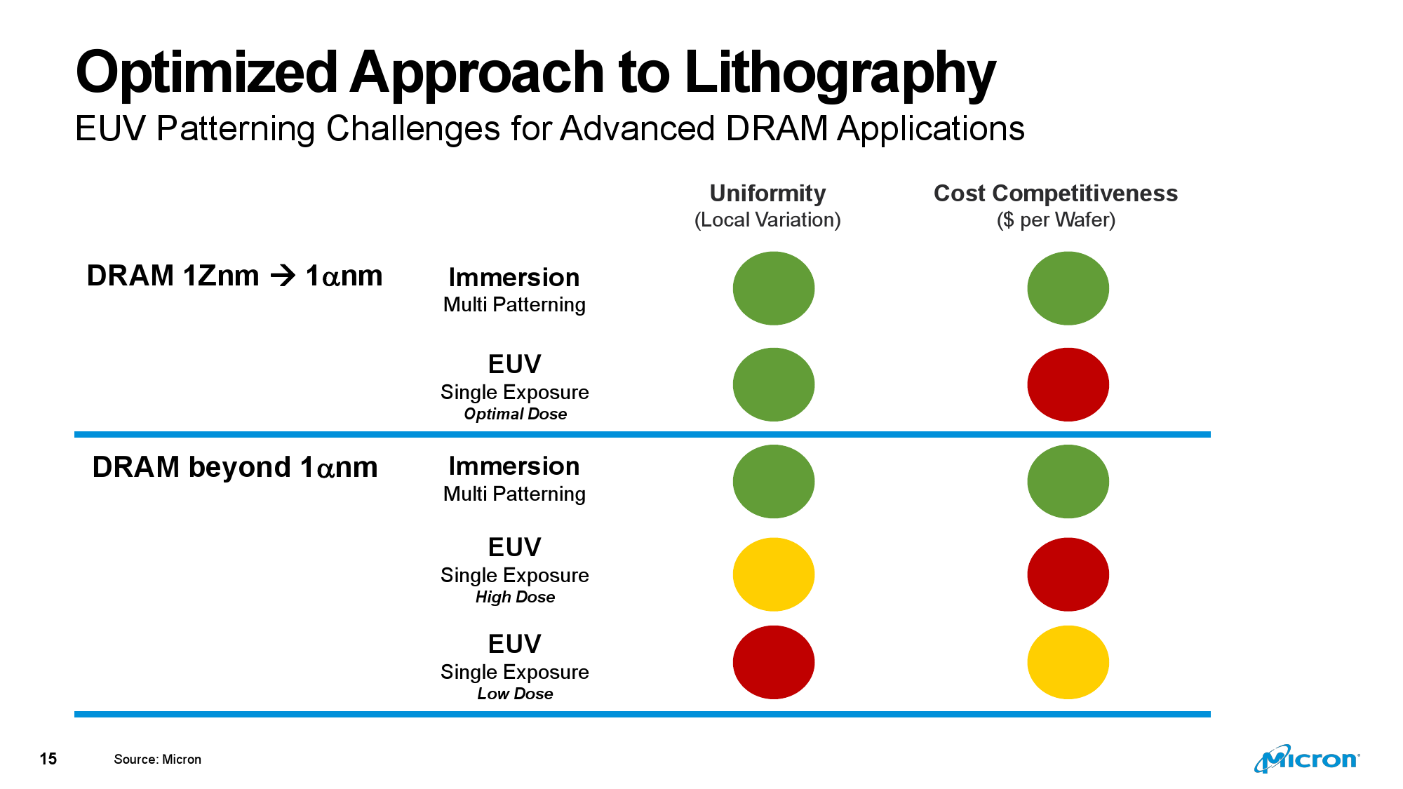
EUV has its challenges not only for logic, but also for DRAM manufacturing when it comes to uniformity and costs. Micron believes that right now EUV tools can only guarantee an acceptable uniformity only when they emit a high dose of EUV radiation (in case of single patterning) which increases wafer costs to unacceptable levels. As such, Micron has no immediate plans to use EUV, but it is closely looking into its evolution and development.
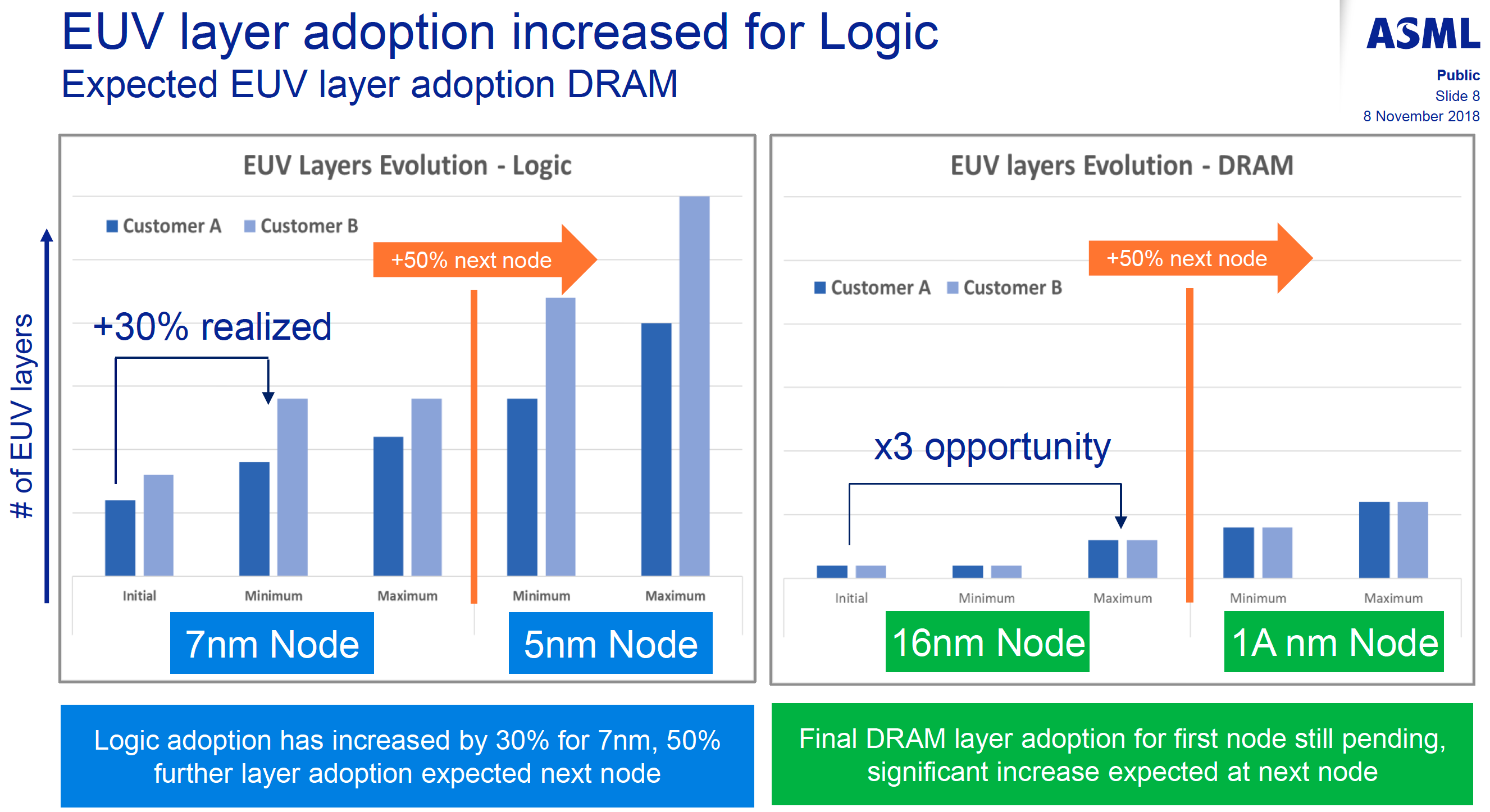
It is highly likely that adoption of EUVL tools by DRAM makers will be similar to that of logic producers (TSMC, Samsung Foundry (which is a contract maker of logic chips, not a DRAM maker)): initially EUV equipment will be used only for a few layers, with the amount of layers increasing gradually with subsequent process nodes. ASML estimates that in case of DRAMs, one EUV layer requires 1.5 to 2 EUV systems for every 100,000 wafer starts per month, so memory makers will need many machines considering their volumes.
It is necessary to note that fabs have to be ready for EUV equipment as these step-and-scan systems are physically larger than DUV tools. This is why SK Hynix is building up a separate fab (called M16) near Icheon, Gyeonggi-do province, that will be EUV ready. We do not know whether Micron’s new cleanrooms will be ready for next-generation lithography equipment.

Some Thoughts
Just several years ago Micron was considerably behind the competition when it came to process technologies. Today, the company is still behind Samsung, but seems to have been able to leapfrog SK Hynix. Based on its new roadmap, the company remains aggressive with its DUV-based nodes, so it will be offer competitive DDR and LPDDR devices to interested parties. Furthermore, development of DDR5 seems to be on track both in terms of technology as well as fabrication process.
Micron is also expanding its DRAM production capacities (which is needed for next-gen processes and next-gen memory), so assuming that its products are good enough, it will be able to maintain its market share going forward. Though, knowing Micron, we understand that the company is more interested in lucrative specialized/disruptive solutions rather than in commodity DRAMs per se.
What looks a little bit disturbing is that Micron seems to be too cautious about EUV lithography. Based on the comments made recently, the company is only evaluating the technology, but (as far as we know) does not invest in cleanrooms ready for EUV. Extreme ultraviolet lithography is not a short or mid-term concern, but it is a little bit strange to see Micron be so shy to talk about it.
Overall, Micron is optimistic about prospects of the DRAM market in general as well as its competitive positions in the future, where various emerging applications (autonomous vehicles, AI/ML, IoT, etc.) are expected to be widely adopted.
Related Reading:
- Micron to Expand Its Fab 6 in Virginia, Build New R&D Center
- Micron Starts Construction of Its Third NAND Fab in Singapore
- Crucial 32 GB DDR4 Modules Found in an ASRock System
- ADATA Demonstrates 32 GB DDR4 Modules, Built on Micron 16 Gb
Sources: Micron, Micron/SeekingAlpha, Micron, Micron, TrendForce, CTimes, Nikkei Asian Review, Electronics Weekly, TechInsights


23 Comments
View All Comments
Jansen - Friday, June 28, 2019 - link
Micron is producing 3200MHz DDR4 unbuffered ECC DIMMs for the new Ryzen chips. Wonder which process generation its using.https://www.micron.com/products/dram-modules/vlp-u...
Jansen - Friday, June 28, 2019 - link
Fixed link:https://www.micron.com/products/dram-modules/vlp-u...
brakdoo - Friday, June 28, 2019 - link
"the company is only evaluating the technology, but (as far as we know) does not invest in cleanrooms ready for EUV"If you don't know, then why make a conclusion???
Is there any reason why the Hiroshima expansion or the new cleanroom in Taichung are not EUV-ready? It's just a height problem.
It would be worth noting that only Hynix is investing in EUV DRAM right now (and only a small portion of their future production). ASML hoped to get more EUV @1Z but Samsung is producing with DUV: https://news.samsung.com/global/samsung-develops-i...
+Techinsights roadmaps are always wrong on timing. just look at their expected timing of previous nodes.
brakdoo - Friday, June 28, 2019 - link
Ok this wasn't intended as a replyArsenica - Friday, June 28, 2019 - link
"Is there any reason why the Hiroshima expansion or the new cleanroom in Taichung are not EUV-ready? It's just a height problem"193i scanners have most of their components located on the production floor but an EUV scanner also uses a significant amount of space in the "basement" to house the laser system needed by the EUV light source.
brakdoo - Friday, June 28, 2019 - link
Yeah, just a height problem...Jansen - Friday, June 28, 2019 - link
More of a depth problem lol. Way easier to add height than to add depth.brakdoo - Friday, June 28, 2019 - link
There is nothing to add if they are building new Fabs anyway.brakdoo - Friday, June 28, 2019 - link
That's a link to a very low profile module.But in general, they have 3200 mhz 1y modules out now, but 1x too...
Jansen - Friday, June 28, 2019 - link
Looks like Micron is only going VLP for 3200MHz ECC unbuffered DIMMs, which makes sense as the premium is negligible and it enables them to cut SKUs.These would be the fastest ECC RAM for Ryzen and ThreadRipper workstations, typically using 64-128GB. Haven't seen anything similar from Samsung yet.