TSMC Unveils N2 Process Node: Nanosheet-based GAAFETs Bring Significant Benefits In 2025
by Anton Shilov on June 16, 2022 3:45 PM EST- Posted in
- Semiconductors
- TSMC
- 2nm
- N2
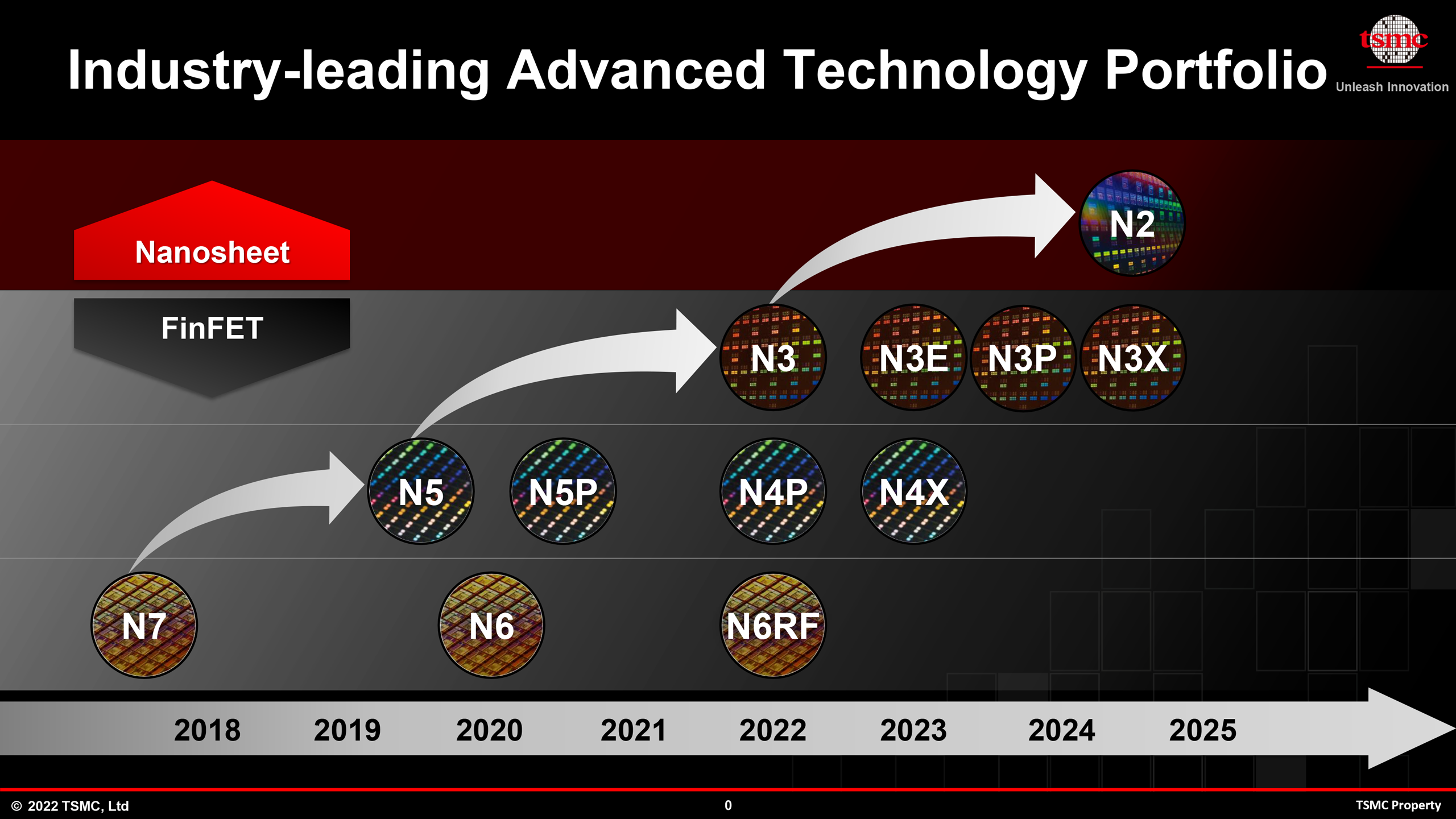
At its 2022 Technology Symposium, TSMC formally unveiled its N2 (2 nm class) fabrication technology, which is slated to go into production some time in 2025 and will be TSMC's first node to use their nanosheet-based gate-all-around field-effect transistors (GAAFETs). The new node will enable chip designers to significantly reduce the power consumption of their products, but the speed and transistor density improvements seem considerably less tangible.
TSMC's N2 is a brand-new platform that extensively uses EUV lithography and introduces GAAFETs (which TSMC calls nanosheet transistors) as well as backside power delivery. The new gate-all-around transistor structure promises well-published advantages, such as greatly reduced leakage current (now that the gates are around all four sides of the channel) as well as ability to adjust channel width to increase performance or lower power consumption. As for the backside power rail, it is generally designed to enable better power delivery to transistors, offering a solution to the problem of increasing resistances in the back-end-of-line (BEOL). The new power delivery is slated to increase transistor performance and lower power consumption.
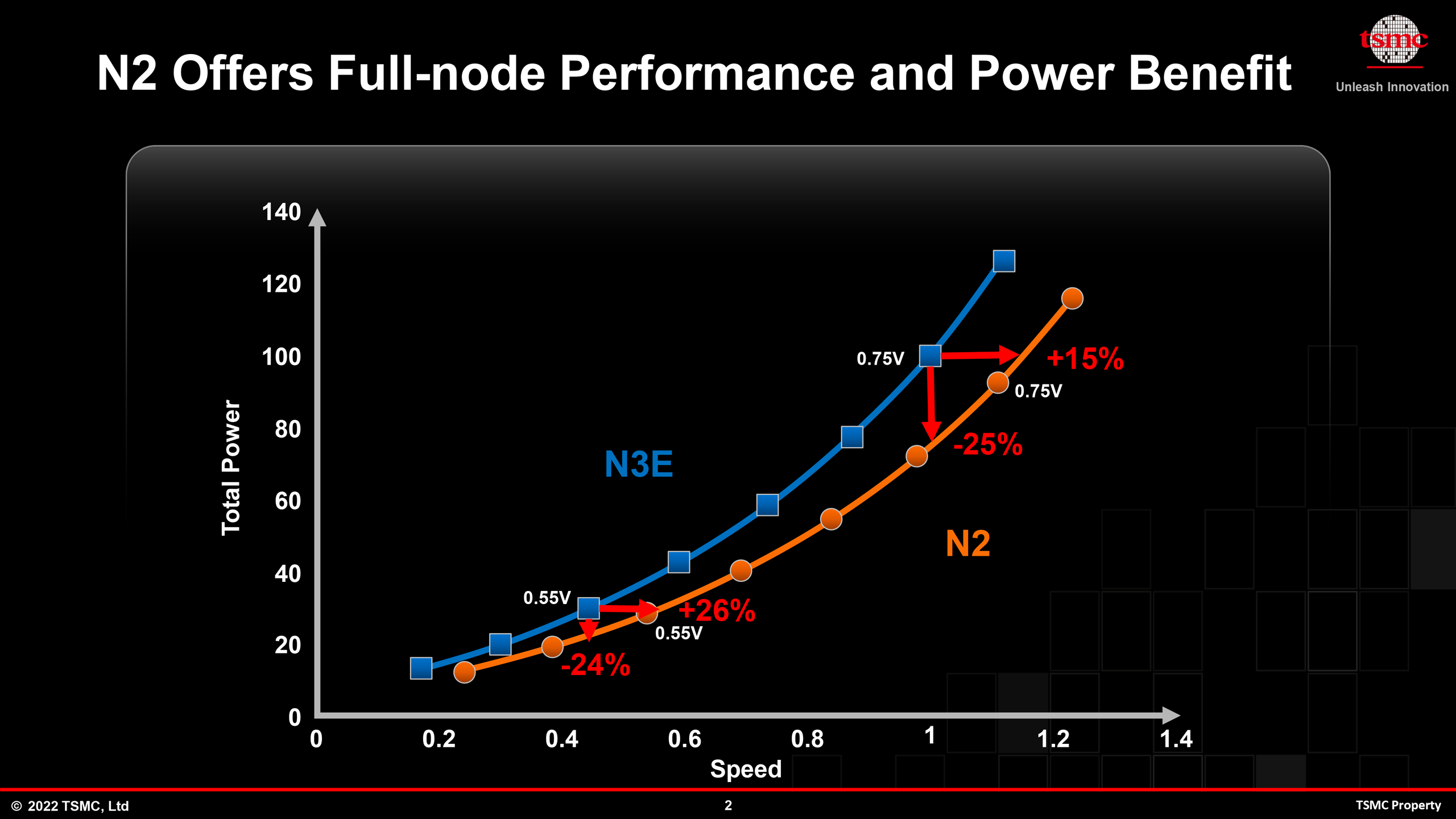
From feature set standpoint, TSMC's N2 looks like a very promising technology. As for actual numbers, TSMC promises that N2 will allow chip designers to increase performance by 10% to 15% at the same power and transistor count, or reduce power consumption at the same frequency and complexity by 25% ~ 30%, all the while increasing chip density by over 1.1-fold when compared to N3E node.
| Advertised PPA Improvements of New Process Technologies Data announced during conference calls, events, press briefings and press releases |
|||||
| TSMC | |||||
| N5 vs N7 |
N3 vs N5 |
N3E vs N5 |
N2 vs N3E |
||
| Power | -30% | -25-30% | -34% | -25-30% | |
| Performance | +15% | +10-15% | +18% | +10-15% | |
| Chip Density* | ? | ? | ~1.3X | >1.1X | |
| Volume Manufacturing |
Q2 2022 | H2 2022 | Q2/Q3 2023 | H2 2025 | |
*Chip density published by TSMC reflects 'mixed' chip density consisting of 50% logic, 30% SRAM, and 20% analog.
Versus N3E, the performance improvements and power reductions enabled by TSMC's N2 node are in line with what the foundry's new nodes typically bring in. But the so-called chip density improvements (which should reflect transistor density gains) are just a little over 10%, which is not particularly inspiring, especially considering that N3E already offers a slightly lower transistor density when compared to vanilla N3. Keeping in mind that SRAM and analog circuits barely scale these days, mediocre improvements in transistor density of actual chips should probably be expected these days. However, a chip density improvement of 10% in about three years is certainly not great news for GPUs and other chips that live or die based on rapidly increasing their transistor counts.
Bearing in mind that by the time TSMC's N2 enters production the company will also have the density-optimized N3S node, it would appear that the foundry will have two process technologies based on different types of transistors yet offering very similar transistor densities, something that has never happened before.
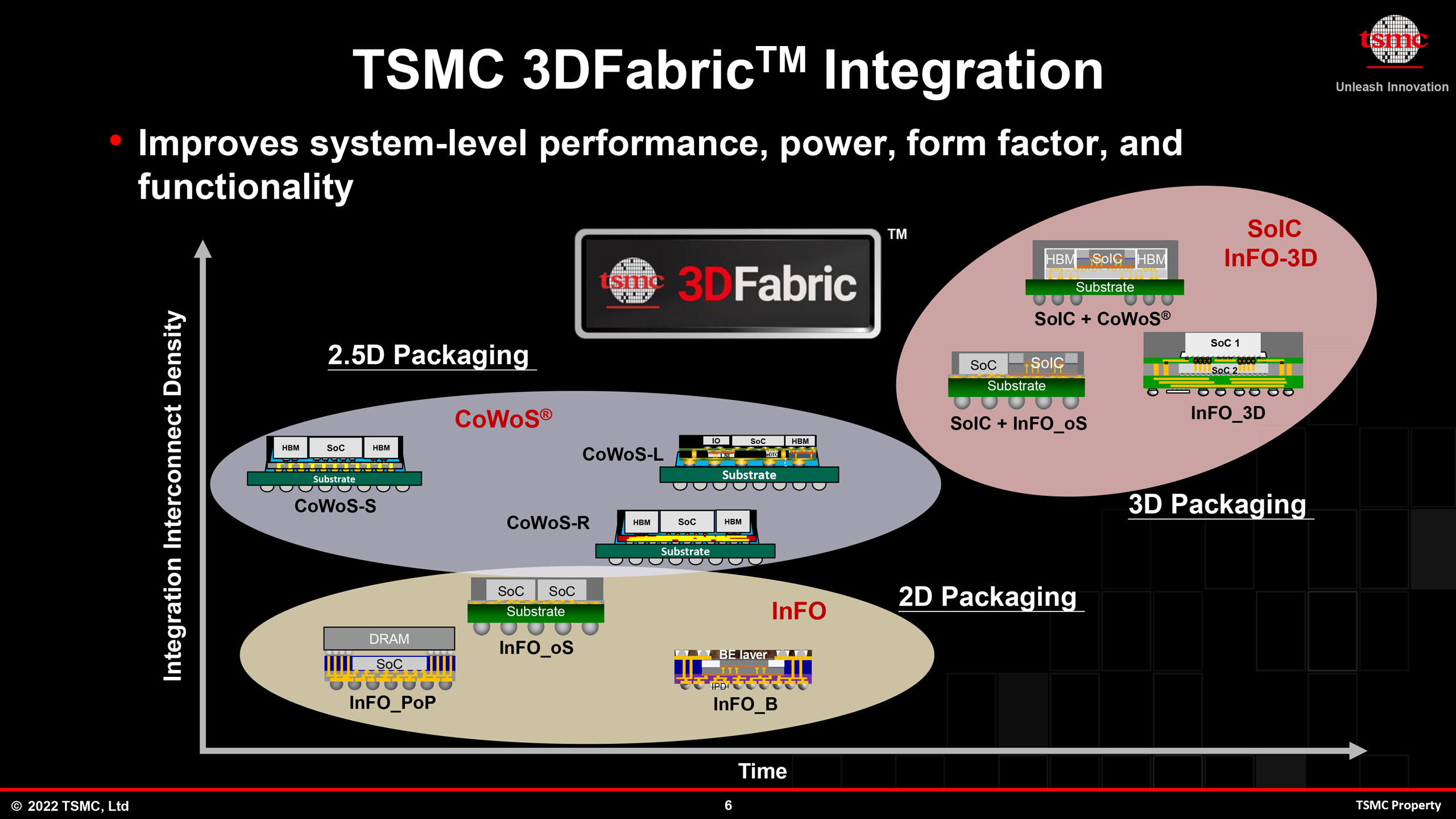
As usual, TSMC will offer their N2 node with various features and knobs to allow chip designers to optimize for things like mobile and high-performance computing designs (note that TSMC calls HPC everything that is not mobile, automotive or specialty. which includes everything from a low-power laptop CPU to a high-end compute GPU aimed at supercomputers). Also, platform offerings include something that TSMC calls 'chiplet integration', which probably means that TSMC enable its customers to easily integrate N2 chips into multi-chiplet packages made using various nodes. Since transistor density scaling is slowing down and new process technologies are getting more expensive to use, multi-chiplet packages are going to become more common in the coming years as developers will be using them to optimize their designs and costs.
TSMC expects to start risk production of chips using its N2 fabrication process sometimes in the second half of 2024, which means that the technology should be available for high volume manufacturing (HVM) of commercial products in the second half of 2025. But, considering the length of modern semiconductor production cycles, it's likely more pragmatic to expect the first N2 chips to become available either very late in 2025 or 2026, if everything goes as planned.


22 Comments
View All Comments
Exotica - Thursday, June 16, 2022 - link
So does intel have a shot (if it doesn’t get delayed along the way) to regain process leadership with 20a and 18a in 2024-25?ballsystemlord - Thursday, June 16, 2022 - link
Intel's current plans are still very aggressive. In the end, they did not even achieve the PPA that they expected to get from 10nm. (Sorry I couldn't find the article about that.)Now currently, they're having problems with their drives for their GPUs...
So, don't count them out, but it's not looking good -- unless you believe their marketing team (Hint: Don't believe marketing.)
ddhelmet - Friday, June 17, 2022 - link
I mean Alder Lake is more efficient than zen 3 and zen 3+ on desktop and mobile. Excluding the beast that is 5950X.Daeros - Friday, June 17, 2022 - link
Are we talking about the same ADL? The one that beats AMD in performance by using double the power? I get that the 12900 is faster than the 5950, but more efficient? This very website shows the 5950x at 137w and the 12900k at 271w.NeuralNexus - Friday, June 17, 2022 - link
Apparently to some numbnuts on this site. INTEL throwing efficiency out of the window to improve performance means they are better than what AMD is able to produce. It's actually kind of hilarious.ddhelmet - Saturday, June 18, 2022 - link
I mean around 30-40W power alder lake is slightly faster no? In gaming and lightly threaded tasks? 12400 is slightly faster than 5600 at same power. Doesn't that make it more efficient? 12700H is faster than 5900HX at the same power. Intel doesn't scale well but because alder lake has higher IPC than Zen 3 it makes it more efficient for certain tasks. Also I specifically said expect 5950X and you still put 5950X on your message. You guys aren't even able to read properly and I'm the numbnut.Soyuzu - Sunday, June 19, 2022 - link
You know that 12700H has 1.75x the core count of 5900HX, and 8 of which are PPA-optimized, right?bananaforscale - Saturday, July 2, 2022 - link
It's you who aren't able to read properly. 5900HX isn't 5900X. It's trivial to get more performance out of same power if you add low power cores. Mobile ADL has more cores than 5900HX. Similarly, I recently replaced the i7-6800K in my NAS with a Haswell Xeon with 12 cores. Result: More multi threaded performance, power draw halved (*measured*, not just TDP).12400 may have the same TDP as a 5600. In reality it will suck more power because AMD's boost works differently.
Wereweeb - Friday, June 17, 2022 - link
TSMC is ahead and tends to deliver on their roadmaps. Intel is behind and tends not to. There's no reason to believe Intel will be ahead of TSMC in the next five years.JKflipflop98 - Thursday, July 7, 2022 - link
You children and your short memories. Intel started the game. They dominated for decades. One little misstep and you kids start rooting for the underdog.Well get your yucks in now squiddo. TSMC's little time in the sun is quickly coming to a close.